MEMS (micro-electromechanical system) microstructure non-contact excitation device based on shock waves

An excitation device, non-contact technology, applied in the direction of microstructure device, microstructure technology, etc., can solve the problems of difficult dynamic characteristic parameters of microstructure, and achieve the effect of good excitation effect, improved vibration excitation ability, and energy concentration.

Inactive Publication Date: 2017-05-10
BOHAI UNIV
View PDF7 Cites 0 Cited by
  • Summary
  • Abstract
  • Description
  • Claims
  • Application Information

AI Technical Summary

Problems solved by technology

However, the main disadvantage of this device is that the device uses an elastic base to excite the microstructure, so when the non-contact optical vibration measurement method is used to test the dynamic characteristics of the microstructure, the vibration response obtained The signal will inevitably contain the vibration response of the base structure, which will make it very difficult to obtain the dynamic characteristic parameters of the microstructure

Method used


Image

  • MEMS (micro-electromechanical system) microstructure non-contact excitation device based on shock waves
  • MEMS (micro-electromechanical system) microstructure non-contact excitation device based on shock waves
  • MEMS (micro-electromechanical system) microstructure non-contact excitation device based on shock waves

Examples


Embodiment Construction

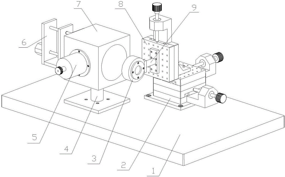
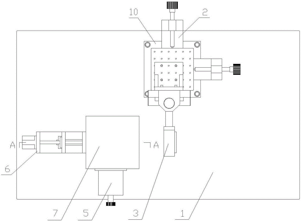
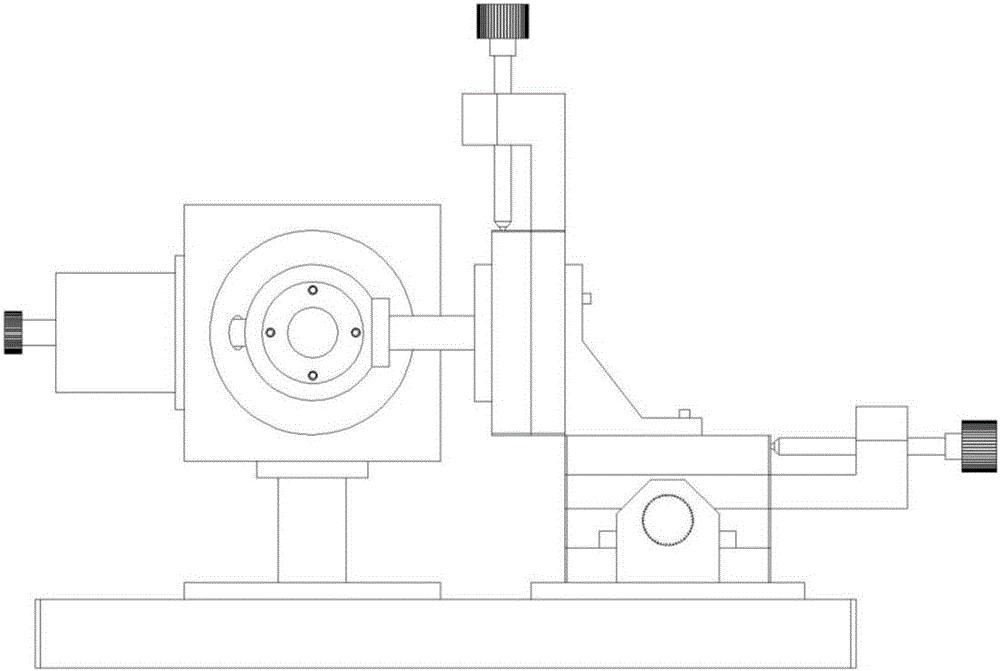
[0030] like Figure 1-Figure 3 As shown, a shock-based MEMS microstructure non-contact excitation device related to the present invention includes a substrate 1, on which a manual three-axis translation platform 2 and a support 4 are arranged, and the manual three-axis translation platform 2 is installed on a bottom plate 10, which is fixed on the base plate 1 by screws. A microstructure unit 3 is provided on the Z-axis slide plate 8 of the manual three-axis displacement table 2;

[0031] like Figure 7-Figure 9 As shown, the microstructure unit 3 includes a mounting sleeve 301 installed on the Z-axis sliding plate 8 through a horizontal support 9, a stepped mounting hole is provided in the mounting sleeve 301, and the bottom of the mounting hole is passed through a micro The structure mounting plate 307 is equipped with a MEMS microstructure 305; the microstructure mounting plate 307 is fixed on the annular plane at the bottom of the mounting hole by the screws 306 uniforml...


PUM


Abstract

The invention discloses an MEMS (micro-electromechanical system) microstructure non-contact excitation device based on shock waves. The device comprises a substrate, a manual three-axis displacement table and a support, wherein a microstructure unit is arranged on the manual three-axis displacement table; an ellipsoidal cavity with an inner cavity in a half ellipsoidal shape is formed at the upper end of the support, a first pin electrode unit is arranged on one side of the ellipsoidal cavity, and the pinpoint of a first pin electrode points to the first focus; the microstructure unit is located at the second focus of the ellipsoidal surface; a second pin electrode unit is arranged on the other side of the ellipsoidal cavity, and the pinpoint of a second pin electrode points to the first focus of the ellipsoidal surface. The first pin electrode and the second pin electrode are electrically connected with two poles of a high-voltage capacitor respectively, and a first air switch is arranged between the high-voltage capacitor and the first pin electrode; the two poles of the high-voltage capacitor are electrically connected to the positive pole and the negative pole of a high-voltage power supply respectively and are controlled to be powered on or off through a second air switch. According to the device, interference of vibration response of a base structure to a test result can be avoided, non-contact type excitation of the MEMS microstructure is realized, and the excitation effect is good.

Description

technical field [0001] The invention belongs to the technical field of micromechanical electronic systems, and in particular relates to a shock wave-based MEMS microstructure non-contact excitation device. Background technique [0002] Due to the advantages of low cost, small size and light weight, MEMS microdevices have broad application prospects in many fields such as automobile, aerospace, information communication, biochemistry, medical treatment, automatic control and national defense. For many MEMS devices, the micro-displacement and micro-deformation of their internal microstructures are the basis for the realization of device functions. Therefore, accurate testing of dynamic characteristic parameters such as the amplitude, natural frequency, and damping ratio of these microstructures has become the key to developing MEMS products. important content. [0003] In order to test the dynamic characteristic parameters of the microstructure, it is first necessary to make ...

Claims


Application Information

Patent Timeline
Patent Type & Authority Applications(China)
IPC IPC(8): B81C99/00
CPCB81C99/0035
Inventor 佘东生杨一柳赵玉峰尹作友赵辉
Owner BOHAI UNIV
Why Eureka
Try Eureka