Silicon carbide semiconductor device

A semiconductor and silicon carbide technology, which is applied in the field of silicon carbide semiconductor devices, can solve the problems of MOSFET gate resistance increase, delay, and polysilicon conductivity is not high enough, and achieve the effect of suppressing breakdown and suppressing the rise of potential

Active Publication Date: 2019-05-21
PANASONIC INTELLECTUAL PROPERTY MANAGEMENT CO LTD
View PDF7 Cites 0 Cited by
  • Summary
  • Abstract
  • Description
  • Claims
  • Application Information

AI Technical Summary

Problems solved by technology

For example, when polysilicon is used as the gate electrode, the conductivity of polysilicon is not high enough, so when the position of the gate electrode is far from the gate pad, the gate resistance of the MOSFET increases
Therefore, in a MOSFET cell with high gate resistance, a delay occurs between the potential of the gate pad and the potential of the gate electrode according to the time constant determined by the gate resistance of the MOSFET and the capacitance between the source and the gate.

Method used


Image

  • Silicon carbide semiconductor device
  • Silicon carbide semiconductor device
  • Silicon carbide semiconductor device

Examples


Embodiment approach

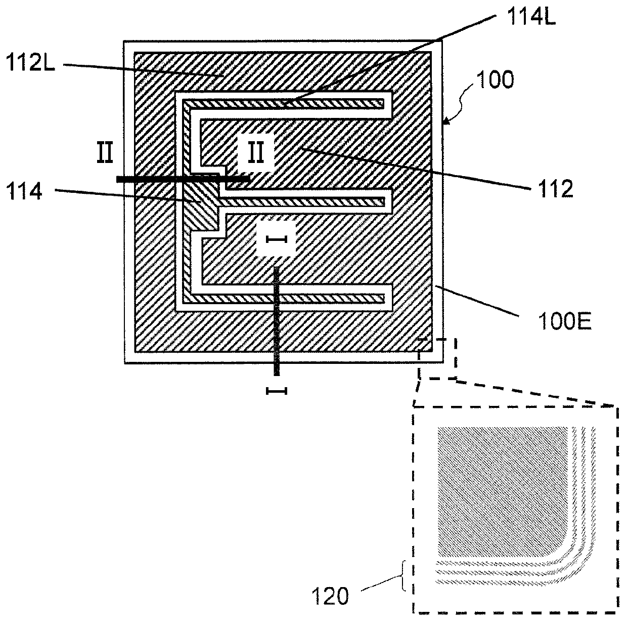
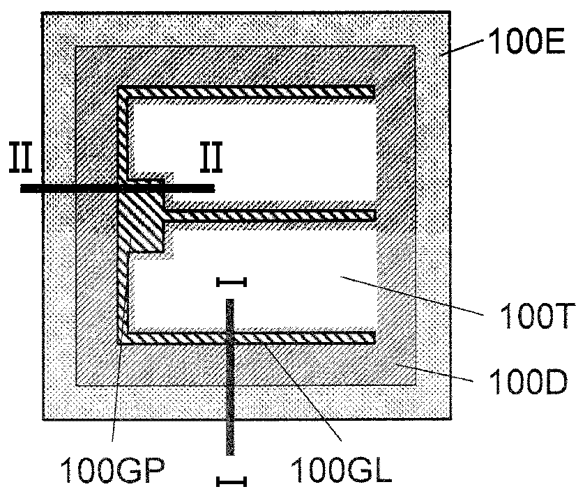
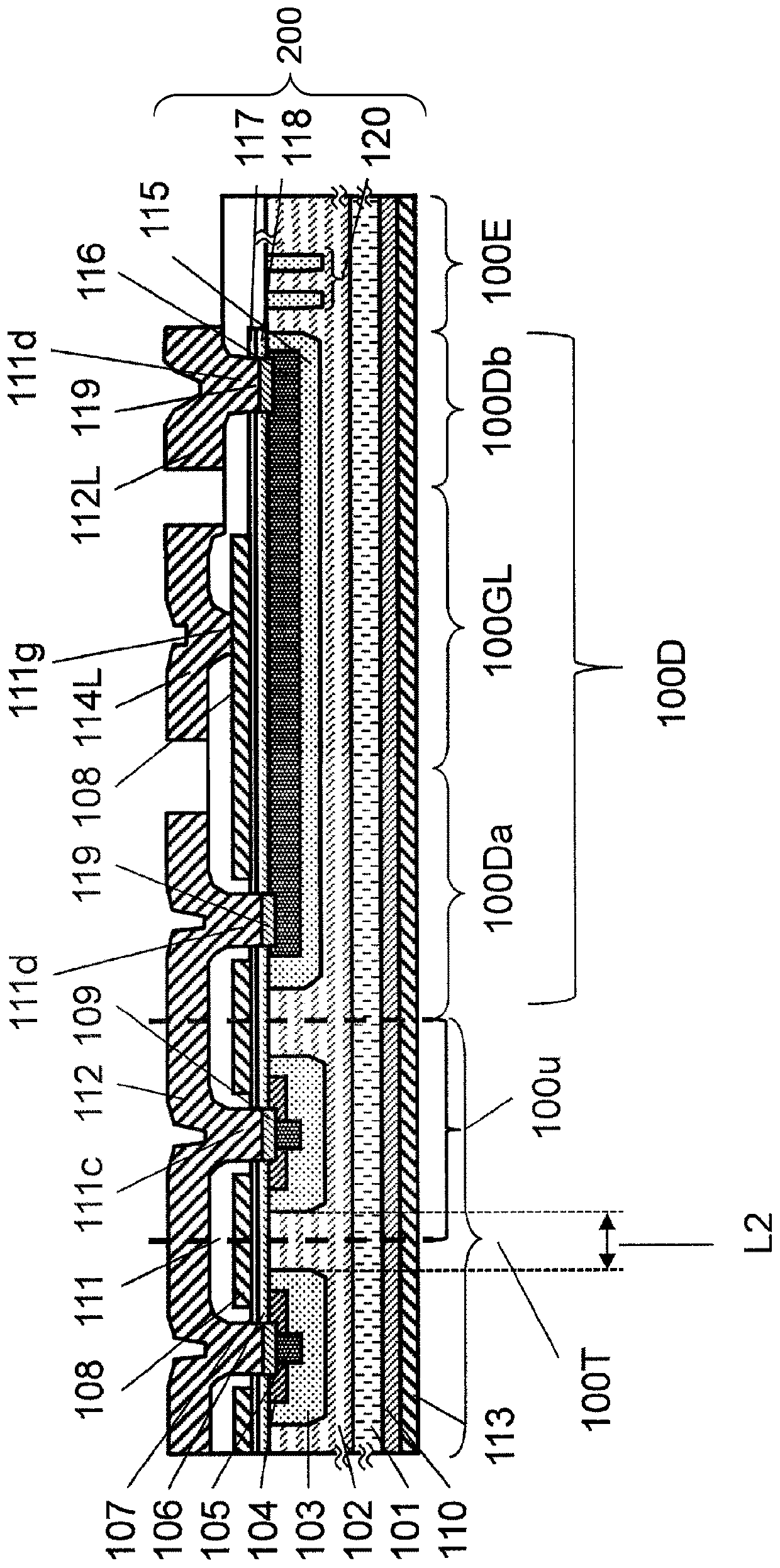
[0069] Referring to Figure 1, figure 2 as well as image 3 Embodiments of the silicon carbide device of this embodiment will be described. Figure 1A It is a schematic plan view of silicon carbide semiconductor device 100 (hereinafter, referred to as SiC-MOSFET 100 ) according to the present embodiment viewed from the principal surface side of the semiconductor substrate. figure 2 yes Figure 1A A schematic cross-sectional view at line I-I is shown, image 3 yes Figure 1A Schematic cross-sectional view at line II-II shown.

[0070]

[0071] SiC-MOSFET 100 of the present embodiment includes stacked structure 200 . The stacked structure 200 includes an n+ type SiC substrate (semiconductor substrate) 101, a drift layer (first silicon carbide semiconductor layer) 102 located on the main surface of the SiC semiconductor substrate 101, and a drain electrode (the first silicon carbide semiconductor layer) located on the back surface of the SiC semiconductor substrate 101. One...

Deformed example 1

[0134] refer to Figure 9 Modification 1 of the semiconductor device of this embodiment will be described.

[0135] As described in the above embodiment, since a large current such as a displacement current or an avalanche current flows through the source wiring of the diode region 100Db, it is preferable to make the width of the source wiring as wide as possible. However, when there is only the diode region 100Db under the upper source wiring, the area other than the transistors in the entire chip increases, the average current amount of the chip area is low, and the on-resistance increases. That is, the area efficiency is poor. Modification 1 is characterized in that a transistor cell is arranged also under the source wiring. Accordingly, it is possible to reduce the decrease in the average current amount of the chip area when the source wiring width is widened.

[0136] Figure 9 A schematic cross-sectional view of Modification 1 of the present embodiment is shown. SiC...

Deformed example 2

[0143] refer to Figure 10 Modification 2 of the semiconductor device of this embodiment will be described.

[0144] Since there is a region thinner than the upper electrode in the upper source wiring 112L, it is preferable to prevent a large current from flowing as much as possible. In particular, in the case of avalanche breakdown, a current equal to the rated current may be discharged from the corner to the outside through the upper source wiring. In SiC-MOSFET 900 according to Modification 2 of the present embodiment, multilayer structure 200 has a substantially quadrilateral shape when viewed from a direction perpendicular to the principal surface of SiC semiconductor substrate 101 . Among the four corners 200a, 200b, 200c, and 200d of the quadrilateral, the withstand voltage of the terminal region 100E in the corners 200a, 200b located closer to the gate pad 114 is at least higher than that in the other two corners 200c, 200d. The withstand voltage of the terminal regi...


PUM


Abstract

The silicon carbide semiconductor device includes a transistor region, a diode region, a gate wiring region, and a gate pad region. The gate pad region and the gate wiring region are respectively arranged so as to be sandwiched by a diode region adjacent to the transistor region and a diode region adjacent to the termination region, and gate electrodes of the gate pad region and the gate wiring region are formed in the region. On the insulating film, the insulating film is formed on the epitaxial layer. This makes it possible to suppress dielectric breakdown of the insulating film in the gate region during switching and avalanche breakdown without degrading the quality of the gate insulating film.

Description

technical field [0001] The present application relates to silicon carbide semiconductor devices. Background technique [0002] Silicon carbide (silicon carbide: SiC) is a semiconductor material having a larger band gap and higher hardness than silicon (Si). For example, SiC is used in power elements such as switching elements and rectifying elements. A power element using SiC has, for example, an advantage of being able to reduce power loss compared to a power element using Si. [0003] A typical semiconductor element using SiC is a metal-oxide-semiconductor field-effect transistor (Metal-Oxide-Semiconductor Field-Effect Transistor: MOSFET). [0004] SiC-MOSFETs are considered to be used, for example, as switching elements used in power converters for driving and controlling loads such as motors. [0005] For example, structures such as those shown in Patent Documents 1 and 2 are disclosed as MOSFETs using SiC. In the MOSFET disclosed in Patent Document 1, an upper sourc...

Claims


Application Information

Patent Timeline
Patent Type & Authority Patents(China)
IPC IPC(8): H01L29/78H01L21/336H01L27/04H01L29/06H01L29/12H01L29/861H01L29/868
CPCH01L27/0727H01L29/8611H01L29/66068H01L29/4238H01L29/7395H01L29/7804H01L29/7811H01L29/0619H01L27/0605H01L29/1608H01L2224/0603H01L29/78H01L27/04H01L29/861H01L29/868H01L29/06H01L29/12H01L29/0623H01L29/41
Inventor 堀川信之楠本修林将志内田正雄
Owner PANASONIC INTELLECTUAL PROPERTY MANAGEMENT CO LTD
Why Eureka
Try Eureka