
Method for preventing wafer map from shifting

A wafer and wafer testing technology, applied in the direction of electronic circuit testing, etc., can solve problems such as deviation and misjudgment of qualified chips.

Active Publication Date: 2017-03-08
BEIJING CHIPADVANCED
View PDF7 Cites 0 Cited by
  • Summary
  • Abstract
  • Description
  • Claims
  • Application Information

AI Technical Summary

Problems solved by technology

Secondly, shift means that the position coordinates of the chip are fixed, but the map coordinates given by the test and the actual results are shifted up and down or left and right, and the test results given will have deviations, such as: X120, Y132 The site test result of the coordinate is bad, and the Map result given after the shift is that the test result of the site of the coordinate is good, which causes a misjudgment of the qualified chip and the failed chip. In order to prevent the multi-chip parallel test process The map shift occurs, how to solve the map shift in the process of multi-site parallel testing is one of the key technical problems to be solved urgently by those skilled in the art

Method used


Image

  • Method for preventing wafer map from shifting
  • Method for preventing wafer map from shifting
  • Method for preventing wafer map from shifting

Examples


Embodiment Construction

[0014] Hereinafter, the present invention will be further described in detail in conjunction with the accompanying drawings: Here, the schematic embodiments of the present invention and their descriptions are used for explanation, but not as a limitation of the present invention.

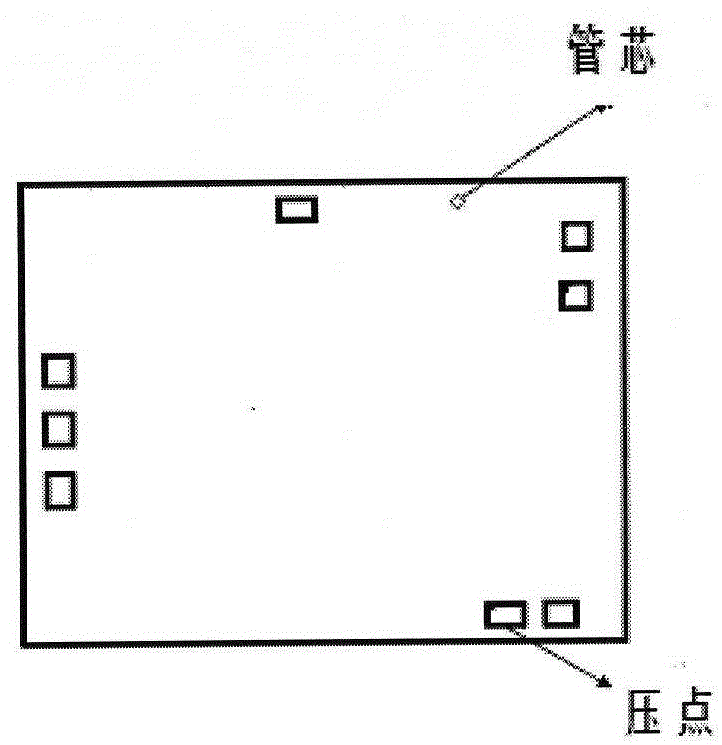
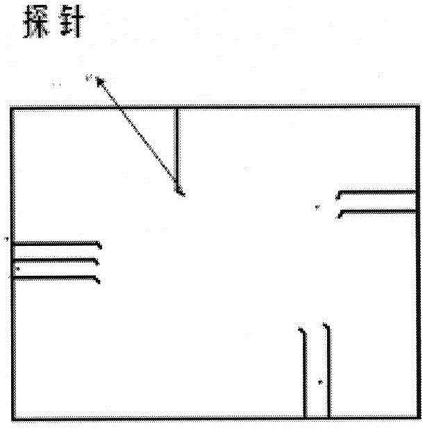
[0015] Take the security chip 16site parallel test as an example, chip pressure points and probes such as figure 1 , 2 shown

[0016] 1. The arrangement of probe cards is 8x2, such as image 3 shown;

[0017] 2. When performing PTPA, set the absolute position of each needle on the probe card when establishing the program. The position of each needle is determined according to the pressure point on a single chip, so as to ensure that each needle will fall on the chip when testing Corresponding pressure point in the middle.

[0018] 3. The default method of detecting cards and needles of the device is AUTO SELECT (automatic selection mode), and the program will automatically set two positioning si...


PUM


Abstract

The invention discloses a method for preventing a map from shifting in the process of wafer test. For PTPA (Probe To Pad Alignment) before wafer test, pins are searched by use of a manual selection mode instead of a conventional method using probe station equipment, and the probes in two farthest specific sites are selected as positioning sites. By using the method, map shifting in the process of multi-site parallel test is avoided. The method is an effective and reliable prevention method.

Description

technical field [0001] The invention relates to a method for preventing a wafer map from shifting, and belongs to the technical field of integrated circuit testing. Background technique [0002] The test of integrated circuit chips is completed by the test system and the probe station through precise docking, and all chips are classified through wafer testing: that is, failed chips and qualified chips. In order to meet the requirements of advanced technology and automation, it is now very Use less ink dots to distinguish good and bad chips, but use an electronic map, which is automatically generated by the probe station during the test. The map not only records whether the chip is good or bad, but also records other test status information of the tested chip; the tested wafer and the electronic map are transmitted to the next process synchronously, for example: input the map, the process's The equipment can automatically complete the operation, and the production line is tr...

Claims


Application Information

Patent Timeline
IPC IPC(8): G01R31/28
Inventor 李亮杨颖超李鑫
Owner BEIJING CHIPADVANCED
Learn More