Touch display device and manufacturing method thereof

A technology of a touch display device and a manufacturing method, which is applied to instruments, electrical digital data processing, and input/output processes of data processing, etc., and can solve problems such as short circuit and affecting the touch performance and display effect of a touch display device 10, To achieve the effect of reducing the resistance value, improving the touch performance and display effect, and the best touch performance

Inactive Publication Date: 2017-03-08
AU OPTRONICS CORP
View PDF0 Cites 7 Cited by
  • Summary
  • Abstract
  • Description
  • Claims
  • Application Information

AI Technical Summary

Problems solved by technology

Thus, Figure 1B The middle part of the second metal layer 142 will be in direct contact with the common electrode layer 16. When the touch display device 10 is powered on, the second metal layer 142 will be short-circuited with the common electrode layer 16, thereby affecting the touch performance of the touch display device 10. and display effect

Method used


Image

  • Touch display device and manufacturing method thereof
  • Touch display device and manufacturing method thereof
  • Touch display device and manufacturing method thereof

Examples


Embodiment Construction

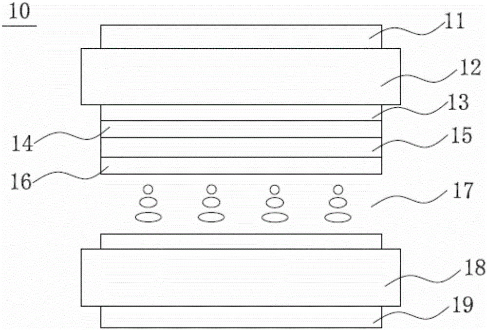
[0027] Below in conjunction with accompanying drawing, structural principle and working principle of the present invention are specifically described:

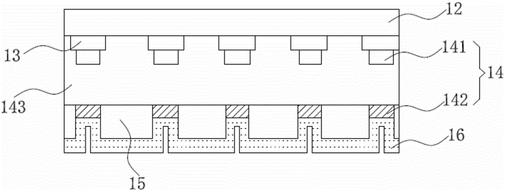
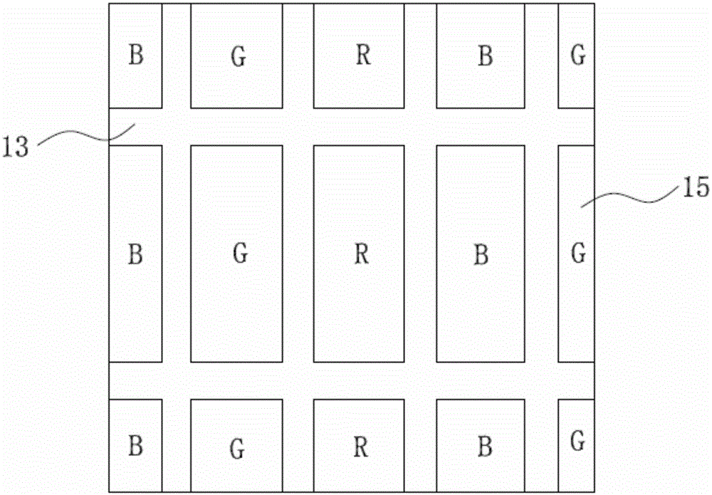
[0028] Please refer to image 3 , Figure 4A ~ Figure 4F and Figure 5A ~ Figure 5F , image 3 It is a schematic flow chart of the manufacturing method of the touch display device of the present invention, Figure 4A ~ Figure 4F It is a partial top view of each step of the manufacturing method of the touch display device in the present invention; Figure 5A ~ Figure 5F for Figure 4A ~ Figure 4F A cross-sectional view along the line AA'.

[0029] The manufacturing method of the touch display device of the present invention is described in detail below, mainly introducing the black matrix layer 1300, the first metal layer 1410, the insulating layer 1430, the second metal layer 1420, the filter film layer 1500 and the common electrode on the upper glass substrate 1200. For the manufacturing method of the layer 1600 and the...


PUM


Abstract

A touch display device and a manufacturing method thereof are provided. The touch display device has a touch sensing area and a virtual touch area, and comprises a first and a second metal layer, filter layers, and common electrode layers. The first metal layer is arranged below an upper glass substrate, and the first metal layer includes a first touch line that is located in the touch sensing area; the second metal layer is arranged below the first metal layer, and includes a second touch line and a second virtual line, wherein the second touch line is located in the touch sensing area, the second virtual line is located in the virtual touch area, and the second touch line and the first touch line form a touch sensing element; the filter layer located in the touch sensing area covers the second touch line, and the filter layer located in the virtual touch area does not cover the second virtual line; and the common electrode layer located in the touch sensing area is not in contact with the second touch line, and the common electrode layer located in the virtual touch area is in direct contact with the second virtual line to reduce the resistance of the common electrode layer. The present invention also discloses a manufacturing method for the touch display device.

Description

technical field [0001] The invention relates to a touch display device and a manufacturing method thereof, in particular to a touch display device capable of reducing the resistance of a common electrode. Background technique [0002] Please refer to Figure 1A and Figure 1B , Figure 1A is a schematic cross-sectional view of an in-cell capacitive touch display device 10 in the prior art, Figure 1B for Figure 1A A schematic cross-sectional view of the upper glass substrate of the middle touch display device 10 . Such as Figure 1A As shown, the touch display device 10 from top to bottom is an upper polarizer 11, an upper glass substrate 12, a black matrix layer 13, a touch sensing element 14, a filter film layer 15, a common electrode layer 16, and a liquid crystal layer. 17. A lower glass substrate 18 and a lower polarizer 19 provided with a thin film transistor array. [0003] Such as Figure 1B As shown, the touch sensing element 14 includes a first metal layer 141...

Claims


Application Information

Patent Timeline
Patent Type & Authority Applications(China)
IPC IPC(8): G06F3/041
Inventor 林韦霖简钰峰郭文瑞
Owner AU OPTRONICS CORP
Why Eureka
Try Eureka