Photo-alignment method, liquid crystal display panel and preparing method thereof

A liquid crystal display panel, photo-alignment technology, applied in optics, nonlinear optics, instruments, etc., can solve problems affecting pixel aperture ratio, transmittance bottlenecks, etc., and achieve the effect of reducing dark lines and improving transmittance.

Inactive Publication Date: 2017-03-15
TCL CHINA STAR OPTOELECTRONICS TECH CO LTD
View PDF8 Cites 5 Cited by
  • Summary
  • Abstract
  • Description
  • Claims
  • Application Information

AI Technical Summary

Problems solved by technology

Swastika shadow pattern seriously affects the aperture ratio of pixels, especially as the number of pixels

Method used


Image

  • Photo-alignment method, liquid crystal display panel and preparing method thereof
  • Photo-alignment method, liquid crystal display panel and preparing method thereof
  • Photo-alignment method, liquid crystal display panel and preparing method thereof

Examples


Example Embodiment

[0032] The implementation of the present invention will be described in detail below with reference to the accompanying drawings and embodiments, so as to fully understand how the present invention applies technical means to solve technical problems and achieve the realization process of technical effects and implement them accordingly. It should be noted that, as long as there is no conflict, each embodiment of the present invention and each feature in each embodiment can be combined with each other, and the technical solutions formed are all within the protection scope of the present invention.

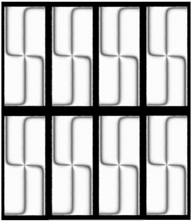
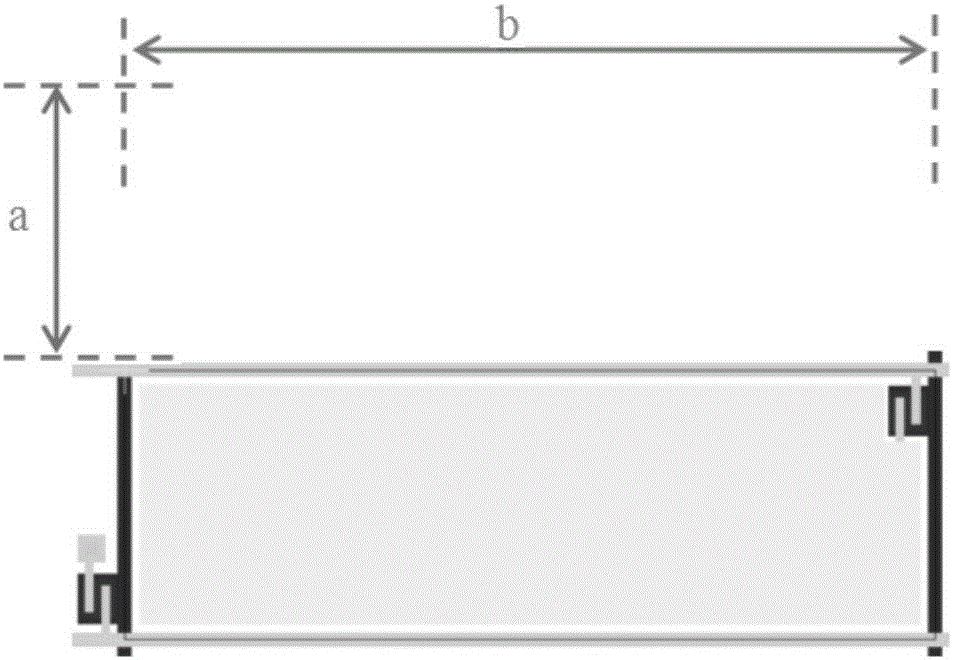
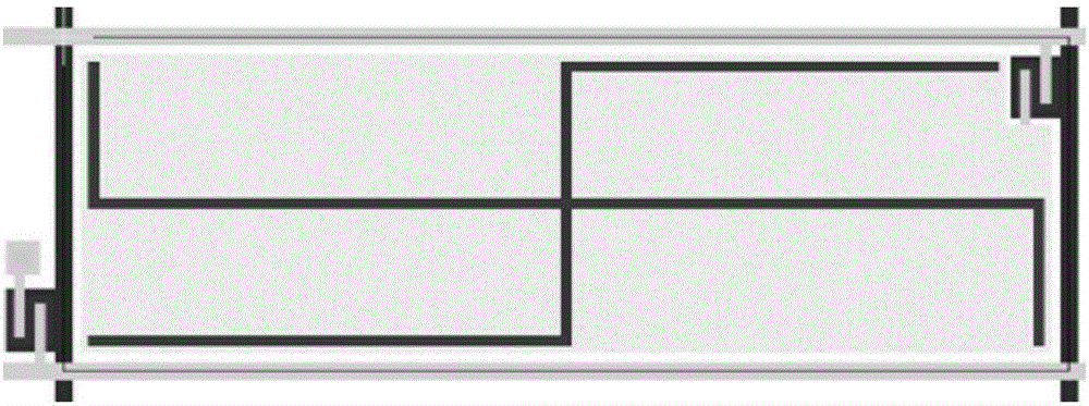
[0033] Such as figure 2 Shown is a schematic top view of a rectangular pixel with the long side b and the wide side a. In the use of traditional optical alignment mode figure 2 When the pixels shown are aligned, the TFT side (ie, the array substrate side) performs up and down exposure alignment along the long side of the pixel, and the exposure width is half of the width of the corres...


PUM


Abstract

The invention provides a photo-alignment method, a liquid crystal display panel and a preparing method thereof. The photo-alignment method includes the steps of performing a first direction exposure with one edge length of a rectangular pixel as exposure width in the photo-alignment process, and performing a second direction exposure with a half of the other edge length of the rectangular pixel as the exposure width. The method can reduce dark fringes on the pixels and improve the transmittance of the display panel.

Description

technical field [0001] The invention belongs to the technical field of manufacturing liquid crystal display panels, and in particular relates to an optical alignment method, a liquid crystal display panel and a manufacturing method thereof. Background technique [0002] In the TFT-LCD production process, there are two liquid crystal alignment methods: rubbing alignment and photo alignment. Rubbing alignment can generate static electricity and particle contamination. Photo-alignment is a non-contact alignment technology that uses linearly polarized light to irradiate the light-sensitive polymer alignment film to form a tilt angle on the polymer alignment film. [0003] In traditional pixel design, light alignment will form "swastika dark pattern" or "swastika dark pattern" inside the pixel, collectively referred to as swastika dark pattern, such as figure 1 shown. Swastika pattern seriously affects the aperture ratio of pixels, especially as the number of pixels per inch o...

Claims


Application Information

Patent Timeline
IPC IPC(8): G02F1/1337
CPCG02F1/133788
Inventor 赵丽
Owner TCL CHINA STAR OPTOELECTRONICS TECH CO LTD
Why Eureka
Try Eureka