Array substrate and display panel with embedded touch structure

An array substrate and display area technology, which is applied in the field of touch control, can solve problems such as large differences in wiring impedance and affect the normal display of display devices, and achieve the effects of improving display quality and uniform common voltage

Active Publication Date: 2019-12-31
WUHAN CHINA STAR OPTOELECTRONICS TECH CO LTD
View PDF5 Cites 0 Cited by
  • Summary
  • Abstract
  • Description
  • Claims
  • Application Information

AI Technical Summary

Problems solved by technology

The common voltage or touch signal transmitted in the driving electrodes and the sensing electrodes is input by the driving chip through the electrode connection lines. The difference in impedance is large, resulting in a large potential difference in the common voltage between the driving electrode and the sensing electrode, which affects the normal display of the display device

Method used


Image

  • Array substrate and display panel with embedded touch structure
  • Array substrate and display panel with embedded touch structure
  • Array substrate and display panel with embedded touch structure

Examples


Embodiment 1

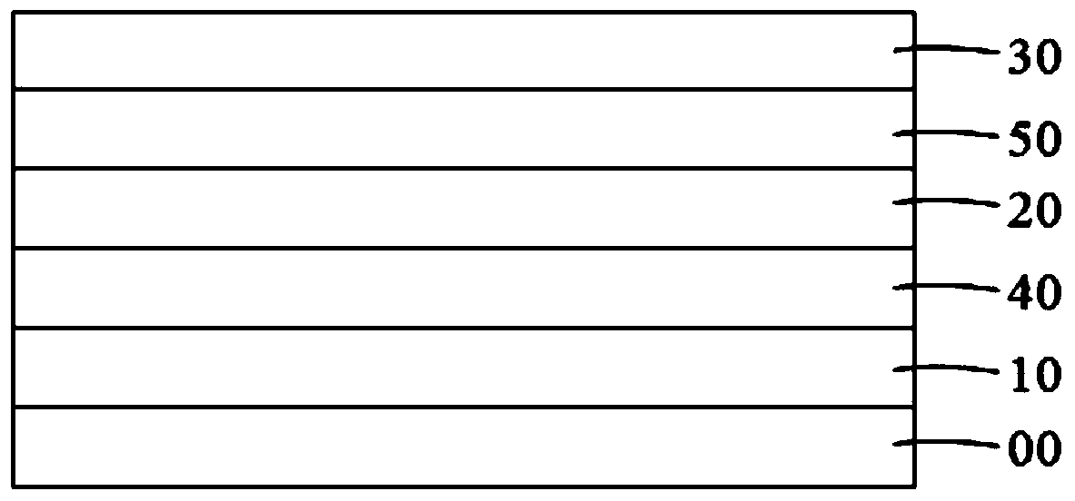
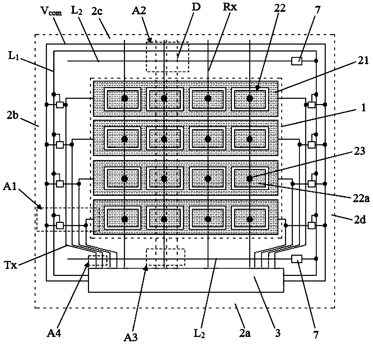
[0029] This embodiment provides an array substrate with embedded touch structure, refer to figure 1 and figure 2 The array substrate includes a data wiring layer 10 , a common electrode layer 20 and a touch wiring layer 30 sequentially disposed on a glass substrate 00 . A first insulating layer 40 is disposed between the pixel structure layer 10 and the common electrode layer 20 , and a second insulating layer 50 is disposed between the common electrode layer 20 and the touch wiring layer 30 .

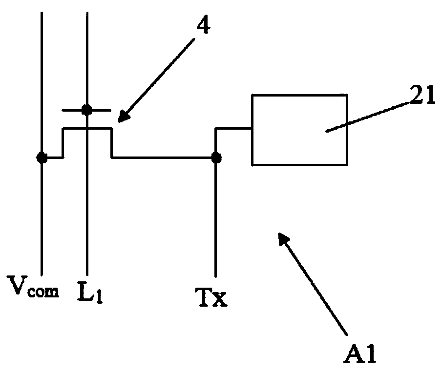
[0030] Among them, such as figure 2 As shown, the data wiring layer 10 is provided with a plurality of parallel data lines D connected to the pixel unit, with figure 23 only exemplarily shows a part of the data line D, and the dotted line indicates that it is located under the common electrode layer 20 . The common electrode layer 20 is divided into a plurality of first electrodes 21 and a plurality of second electrodes 22 extending perpendicular to each other and insulated from ...

Embodiment 2

[0044] This embodiment firstly provides a display panel, such as Figure 7 As shown, the display panel is a liquid crystal display panel, which includes an array substrate 100 and a color filter substrate 200 disposed opposite to each other, and a liquid crystal layer 300 is filled between the array substrate 100 and the color filter substrate 200, wherein the array substrate 100 is an array substrate embedded with a touch structure as provided in Embodiment 1 above.

[0045] Another aspect of this embodiment is a display device, such as Figure 8 As shown, the display device includes a display panel 400 and a backlight module 500, the display panel 400 is arranged opposite to the backlight module 500, and the backlight module 500 provides a display light source to the display panel 400, so that The display panel 400 displays images. Wherein, the display panel 400 adopts the liquid crystal display panel provided in this embodiment.

[0046]To sum up, in the array substrate ...


PUM


Abstract

An array substrate having an embedded touch structure is disclosed. A common electrode layer is divided in to multiple first and second electrodes. Multiple first and second electrode connecting lines disposed in a touch wiring layer are respectively connected the first and second electrodes to a driving integrated chip one by one. A common voltage signal line, a first switching signal line and a first and second switches are disposed in a layout area. In a display sequence, the first switching signal controls the first and second switches to turn on, so the first and second electrode connecting lines are respectively connected to the common voltage signal line. In a touch sequence, the first switching signal controls the first and second switches to turn off to disconnect the first and second electrode connecting lines and the common voltage signal line. A display panel having the array substrate is also disclosed.

Description

technical field [0001] The present invention relates to the field of touch technology, in particular to an array substrate and a display panel embedded with a touch structure. Background technique [0002] As an input medium, the touch display screen is currently the simplest and most convenient way of human-computer interaction, so the touch display screen is more and more applied to various electronic products. Based on different working principles and information transmission media, touch screen products can be divided into four types: infrared touch screen, capacitive touch screen, resistive touch screen and surface acoustic wave touch screen; among them, capacitive touch screen has long life, high light transmittance, and can support multiple Point touch and other advantages have become the current mainstream touch screen technology. Capacitive touch screens include surface capacitive and projected capacitive, and projected capacitive can be further divided into self-c...

Claims


Application Information

Patent Timeline
Patent Type & Authority Patents(China)
IPC IPC(8): G06F3/041G06F3/044G02F1/1333G02F1/1362
CPCG02F1/13338G02F1/136286G06F3/0412G06F3/0416G06F3/044G06F2203/04111G06F3/0443G02F1/13306G02F1/133514G02F1/134309G02F1/13439G02F1/1368G02F2201/121
Inventor 张启沛陈彩琴
Owner WUHAN CHINA STAR OPTOELECTRONICS TECH CO LTD
Why Eureka
Try Eureka