
Display panel and display device thereof

A technology for display panels and display areas, applied in static indicators, optics, instruments, etc., to solve problems such as slow voltage recovery, uneven common voltage in the display area, and large screen edge differences

Inactive Publication Date: 2019-12-20
WUHAN CHINA STAR OPTOELECTRONICS TECH CO LTD
View PDF7 Cites 0 Cited by
  • Summary
  • Abstract
  • Description
  • Claims
  • Application Information

AI Technical Summary

Problems solved by technology

The common electrode will be coupled by the scan line, data line, and pixel electrode. During the display process, the voltage on the common electrode is constantly changing. Due to the high resistivity of ITO, the part of the common electrode close to the common wiring is subject to coupling. After the voltage recovery is faster, the common electrode in the center of the display area recovers slowly after being coupled, which will make the common voltage of the display area uneven
When the public voltage of the display area is uneven, the difference between the Best Vcom (the Vcom that minimizes the screen flicker) between the edge of the screen and the center of the screen is large, resulting in flickering around the screen

Method used


Image

  • Display panel and display device thereof
  • Display panel and display device thereof
  • Display panel and display device thereof

Examples


Embodiment 1

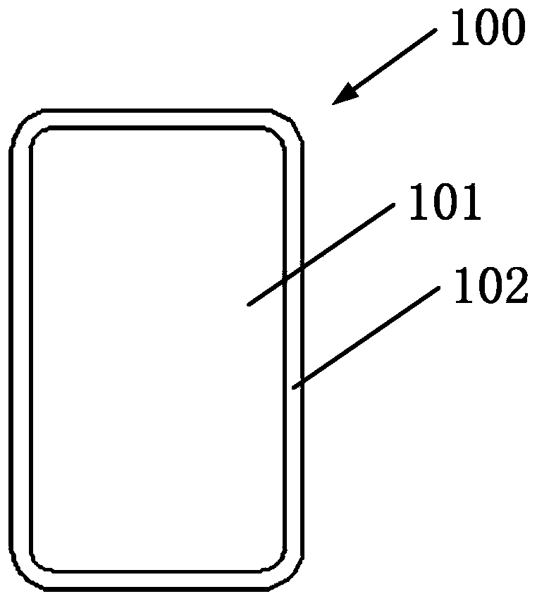
[0041] Such as figure 1 As shown, a display panel 100 is defined with a display area 101 and a non-display area 102 surrounding the display area 101 .

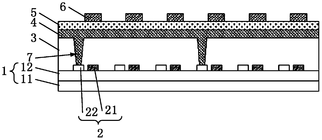
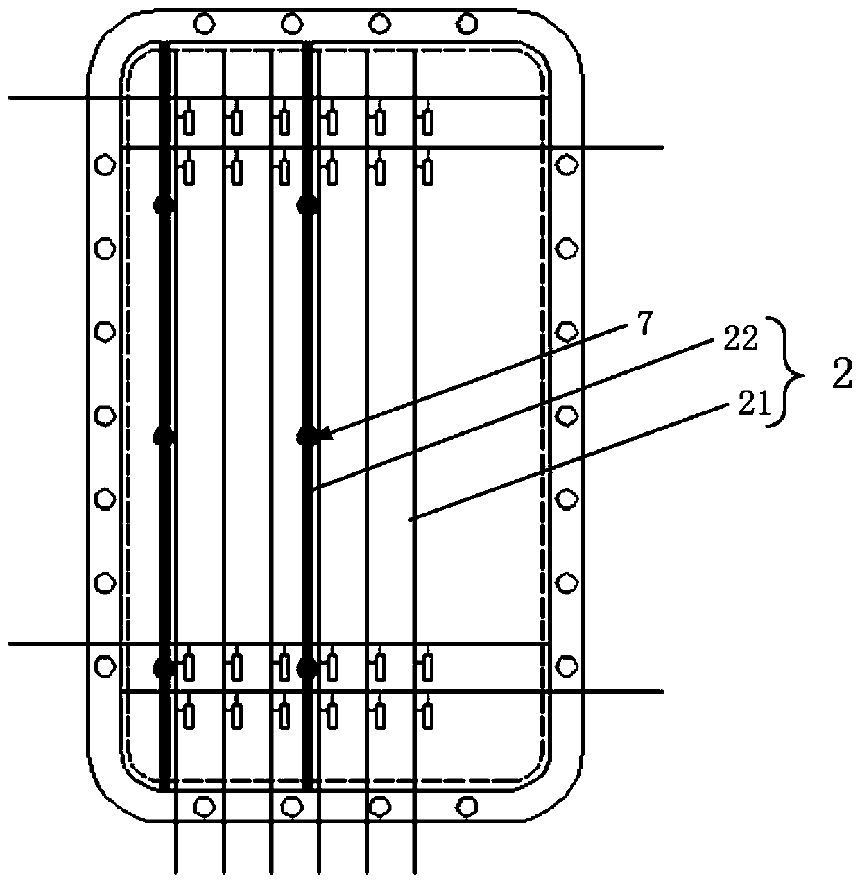
[0042] Such as figure 2 , image 3 As shown, the display panel 100 in the display area 101 includes: a base layer 1 , a metal layer 2 , a flat layer 3 , a common electrode layer 4 , an insulating layer 5 and a pixel electrode layer 6 . The base layer 1 includes a substrate 11 and a functional layer 12 disposed on the substrate 11 . The functional layer 12 includes a buffer layer, an active layer, a gate insulating layer, a gate layer, an interlayer insulating layer and other structures sequentially disposed on the substrate 11 , which will not be described in detail here.

[0043] Such as figure 2 , image 3 As shown, wherein the metal layer 2 is disposed on the base layer 1 . Wherein the metal layer 2 includes: data wires 21 and common wires 22 . Wherein the data wires 21 are arranged parallel to each other at interv...

Embodiment 2

[0051] The schematic plan view of the display panel 100 described in this embodiment and figure 1 Similar, so no more details.

[0052] Such as Figure 4 , Figure 5 As shown, the difference between this embodiment and the display panel 100 described in Embodiment 1 is that in this embodiment, a common wire 22 is arranged in parallel with the same layer of metal on one side of each data wire 21, so that the display area The common voltage of 101 becomes uniform, reducing the Best Vcom difference between the edge of the screen and the center of the screen, and improving the flickering phenomenon around the screen.

Embodiment 3

[0054] Such as Figure 6 As shown, the display panel 100 in this embodiment is a horizontal screen display. The structural schematic diagram of the display panel 100 in the display area 101 described in the embodiment and figure 2 are similar, so they will not be repeated here.

[0055] Such as Figure 7 As shown, the difference between this embodiment and the display panel 100 described in Embodiment 1 is that the display panel 100 described in this embodiment is suitable for medium-sized screens, while the display panel 100 of Embodiment 1 is suitable for small-sized screens. In other words, the display panel of Embodiment 1 is a vertical screen display, while the display panel 100 of this embodiment is a horizontal screen. Specifically, a screen below 8 inches may be defined as a small-size screen, and a screen above 8 inches may be defined as a medium-size screen.

[0056] Likewise, in this embodiment, common wirings 22 are arranged in parallel on one side of the data...


PUM


Abstract

The invention discloses a display panel and a display device thereof. A common line is arranged in parallel on one side of a data line of a display area, and the common line is connected to a common electrode layer through a via hole. Thus, the common voltage of the display area is enabled to become uniform; the Best Vcom difference between the screen edge and the screen center is reduced; and thephenomenon of peripheral flickering of the screen is improved.

Description

technical field [0001] The present invention relates to the field of display technology, in particular to a display panel and a display device thereof. Background technique [0002] The display device can convert the data of the computer into various characters, numbers, symbols or intuitive images and display them, and can use keyboard and other input tools to input commands or data into the computer, and add, delete, modify and change the display at any time with the help of the system's hardware and software. content. Display devices are classified into plasma, liquid crystal, light emitting diode, and cathode ray tube according to the display device used. [0003] LCD (English full name: Liquid Crystal Display, liquid crystal display). The liquid crystal display uses liquid crystal material as the basic component, fills the liquid crystal material between two parallel plates, and changes the alignment of the molecules inside the liquid crystal material through voltage ...

Claims


Application Information

Patent Timeline
IPC IPC(8): G02F1/1362G06F3/041
CPCG02F1/136286G02F1/13338G06F3/0412G09G3/3648
Inventor 杨跃骅
Owner WUHAN CHINA STAR OPTOELECTRONICS TECH CO LTD
Learn More