Light guide plate, backlight module group and optical microstructure processing method

A technology of optical microstructure and processing method, which is applied in the field of optical components, can solve the problems of increasing the processing time, increasing the volume of the mold core, and impracticable production, etc., so as to improve the uniformity of light output, uniform light output efficiency, and improve process efficiency and The effect of precision

Active Publication Date: 2017-03-29
苏州茂立光电科技有限公司
View PDF5 Cites 4 Cited by
  • Summary
  • Abstract
  • Description
  • Claims
  • Application Information

AI Technical Summary

Problems solved by technology

The above-mentioned injection molding and tool engraving are only suitable for making small-sized light guide plates. The reason is that when the size of the light guide plate becomes larger, the number of microstructures arranged on it will also increase. If a large-sized light guide plate is made by injection, The volume of the corresponding mold core will be greatly increased, and it is impossible to implement it in production
However, if the tool is used to directly mark the microstructure on the light guide plate, in addition to increasing the processing time due to the number of microstructures, compared with the small-sized light guide plate, the processing of the broken knife is more likely to occur. For reprocessing after the knife is broken The influence of the tool's return accuracy is inevitable

Method used


Image

  • Light guide plate, backlight module group and optical microstructure processing method
  • Light guide plate, backlight module group and optical microstructure processing method
  • Light guide plate, backlight module group and optical microstructure processing method

Examples


Embodiment 1

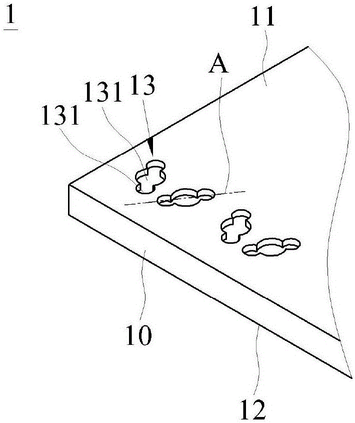
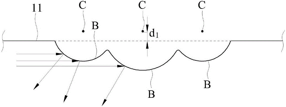
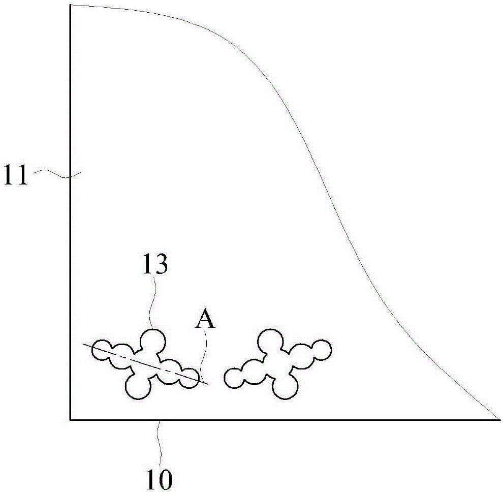
[0078] Please combine Figures 1 to 4 It should be understood that it is a three-dimensional schematic view of the light guide plate, a schematic cross-sectional view of the optical microstructure, and a schematic plan view of each light guide plate in Embodiment 1 of the present invention. The present invention discloses a light guide plate 1 comprising a light incident surface 10 , a light exit surface 11 , a bottom surface 12 and several optical microstructures 13 .

[0079] The light incident surface 10 is used to receive light from a light source (not shown in the figure). The light exit surface 11 and the bottom surface 12 are opposite to each other and vertically adjacent to the light incident surface 10 . The optical microstructures 13 are formed on the light-emitting surface 11 or the bottom surface 12 of the light guide plate 1 , and here the optical microstructures 13 are formed on the light-emitting surface 11 as an example. Any optical microstructure 13 has sever...

Embodiment 2

[0085] Such as Figure 8 , 9a As shown in and 9b, it is a schematic diagram of the steps of Embodiment 2 of the present invention and a schematic partial cross-sectional view of the optical microstructure. The present invention also discloses a processing method of an optical microstructure, comprising the following steps:

[0086] Step S01 : providing a substrate 4 with a processed surface 40 .

[0087] Step S02: using a laser beam S with a first power 1 Bombard the processing surface 40 to form a first recess 401, such as Figure 9a shown.

[0088] Step S03: using a laser beam S with a second power 2 Bombard the processing surface 40 to form a second cavity 402, and the first cavity 401 and the second cavity 402 intersect to form an optical microstructure 41, such as Figure 9b As shown, however, the laser beam S with the first power shown in the figure 1 and the laser beam S with the second power 2 For illustration only. Specifically, in the process of forming the ...

Embodiment 3

[0092] Such as Figure 10 and 11 As shown, it is a flow chart of the steps and a schematic diagram of the optical microstructure of Embodiment 3 of the present invention. In this embodiment, after passing the laser beam S with the first power 1 Bombarding the processing surface 40 or passing a laser beam S with a second power 2 After bombarding the processing surface 40, step S04 is also included: using a laser beam with a third power to bombard the processing surface 40 to form a third cavity 403, and the third cavity 403 intersects with the first cavity 401 to form an optical microstructure 41, here to utilize the laser beam S with the second power 2 After bombarding the processing surface 40 , the laser beam with the third power is used to bombard the processing surface 40 as an example. In this way, the optical microstructure 41 formed on the processed surface 40 can form a cross shape or a triangle shape in plan view, such as Figure 11 As shown in the figure, the op...


PUM


Abstract

The invention provides a light guide plate, a backlight module group and an optical microstructure processing method. An optical microstructure having a number of continuous arc recessed parts is arranged on the light guide plate, a section of the optical microstructure is shaped as a number of connected arc line segments, neighboring arc recessed parts are not equal in maximum depth, and therefore the optical microstructure is enabled to have a long axis. Via the optical microstructure, light rays reaching the light guide plate are enabled to proceed along the long axis, a dark zone of the light guide plate can be filled with the light rays, and overall light emitting uniformity can be improved. Demand for large-sized light guide plates can be satisfied because the optical microstructure can be processed via laser, and light guide plates with high yield rate s can be provided.

Description

technical field [0001] The invention relates to the field of optical components, in particular to a light guide plate, a backlight module and an optical microstructure processing method. Background technique [0002] In view of the excellent optical characteristics of the light guide plate, it has been widely used as the main light guide component of the backlight module in the display in recent years, so that the incident light can form a uniform surface light source and provide it to the panel. [0003] In order to destroy the total reflection phenomenon caused by light incident on the light guide plate, microstructures are designed on the light guide plate to adjust the light uniformity or change the light path. In addition to the microstructure used to make the light emit light on the light guide plate to form a surface light source, since today’s backlight modules have mostly used light-emitting diodes (hereinafter referred to as LEDs) as the light source, the light emi...

Claims


Application Information

Patent Timeline
Patent Type & Authority Applications(China)
IPC IPC(8): G02B6/00
CPCG02B6/0038G02B6/0065
Inventor 廖崑廷
Owner 苏州茂立光电科技有限公司
Why Eureka
Try Eureka