Lighting device

a technology of light source and light source, which is applied in the direction of lighting and heating equipment, semiconductor devices for light sources, instruments, etc., can solve the problems of long life span, limited thickness of entire products, and inability to easily change product plans and designs, etc., to achieve stable brightness, high reliability, and high heat resistance resin

Active Publication Date: 2013-12-19
LG INNOTEK CO LTD
View PDF2 Cites 38 Cited by
  • Summary
  • Abstract
  • Description
  • Claims
  • Application Information

AI Technical Summary

Benefits of technology

[0017]Also, still further advantageous effect according to the embodiments of the present invention is that the resin layer is formed of high heat resistant resin so that, in spite of the heat generated from the light source package, stable brightness can be implemented and the lighting device having high reliability can be provided.
[0018]Moreover, still further advantageous effect according to the embodiments of the present invention is that the lighting device is formed using the flexible printed circuit board and the resin layer so that flexibility can be secured, thereby enabling a degree of freedom in product design to be improved.
[0019]Furthermore, still further advantageous effect according to the embodiments of the present invention is that the diffusion plate itself surrounds a side surface of the light source module so that the diffusion plate itself can perform the function of a housing, and thus as a separate structure is not used, manufacturing process efficiency and, durability and reliability of the product itself can be improved. Also, according to the embodiments of the present invention, heat dissipation efficiency can be improved and a wavelength shift and a reduction in illumination intensity can be controlled.
[0020]Also, still further advantageous effect according to the embodiments of the present invention is that the light reflection member is provided so that the light loss generated from the side surface of the resin layer can be minimized, thereby enabling brightness and roughness of the lighting device to be improved.
[0021]Also, still further advantageous effect according to the embodiments of the present invention is that the reflection unit having the spacing part is provided on the surface of the printed circuit board so that the improvement of light reflectance as well as the improvement of brightness can be maximized. Furthermore, although the thickness of the lighting device and the number of the light source are not increased, the brightness can be improved, and thanks to a pattern design of the separation member (i.e. a spacer) which forms the spacing part, the control of light and reflection efficiency can be maximized.
[0022]Also, still further advantageous effect according to the embodiments of the present invention is that the optical pattern layer is formed in the light source module so that the concentration of light and the generation of a hot spot can be inhibited, and the uniformity of light supplied to the diffusion plate can be improved.

Problems solved by technology

Unlike a florescent lamp, since the LEI) device does not use harmful substances such as mercury and the like, it has a low possibility to cause environmental pollution and a long life span compared to a conventional light source.
However, due to a thickness of the tight guide plate itself, there is a limitation to make the thickness of an entire product thin.
Furthermore, as a material of the light guide plate is not flexible, it is disadvantageous that it would be difficult to apply the light guide plate to a part in which a bend is formed, and thus a product plan and design cannot be easily changed.
Also, as the light is partially emitted to the side of the light guide plate, light loss is generated.
Thus, it is problematic that light efficiency is reduced.
Furthermore, as a temperature of the LEDs increases at the time of light emission, it is also problematic that the LEDs' characteristics (e.g. luminous intensity and wavelength transition) are changed.

Method used


Image

  • Lighting device
  • Lighting device
  • Lighting device

Examples


second exemplary embodiment

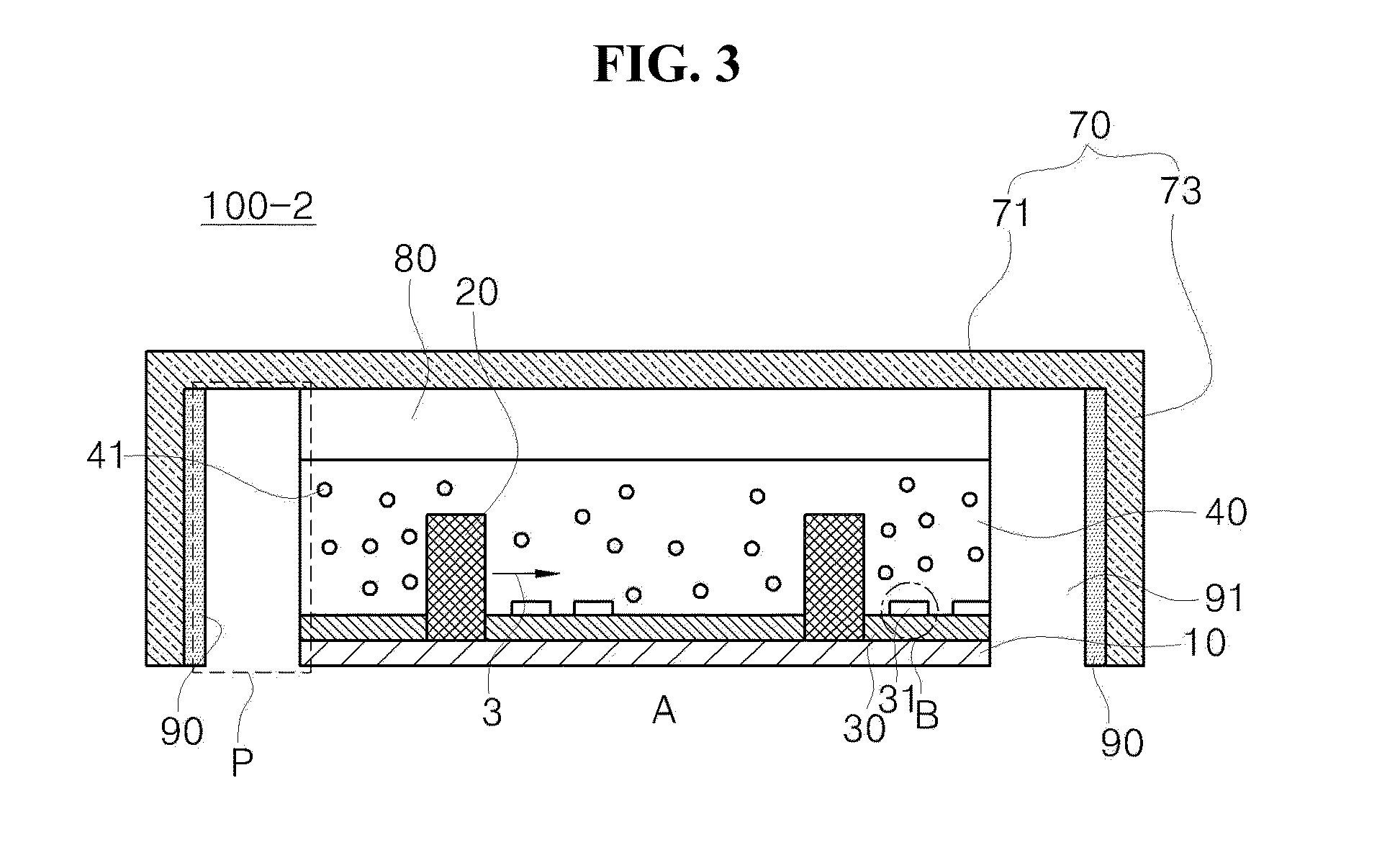
[0121]FIG. 7 illustrates a structure in which the heat dissipation member 110 is added to the light source module 100-1 of FIG. 2. However, it would also be obvious to those having ordinary skill in the art that the heat dissipation member can be also added to the light source modules 100-2, 100-3 of FIG. 3 and FIG. 6 which are the second exemplary embodiment and the third exemplary embodiment.

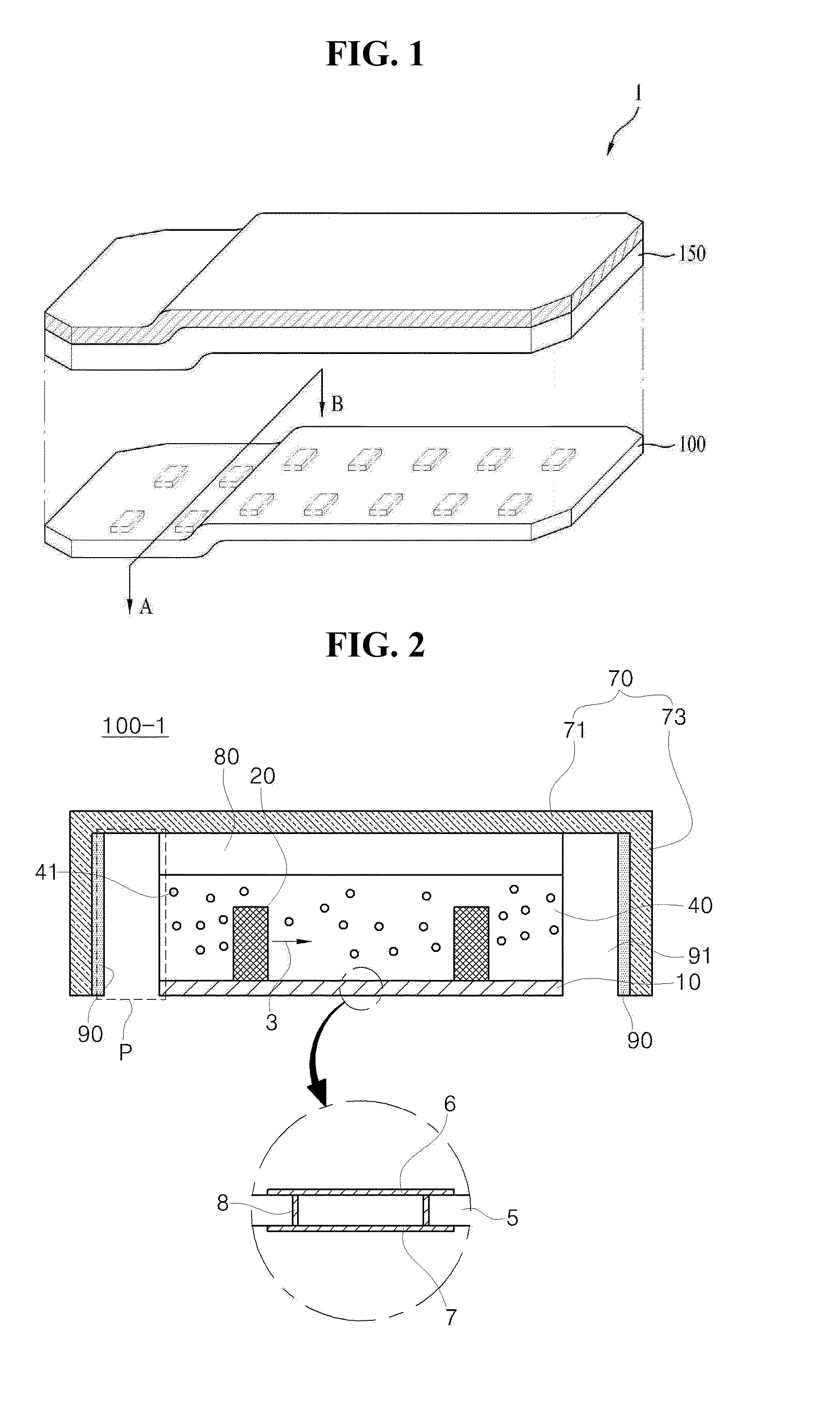
[0122]FIG. 8 shows a fifth exemplary embodiment 100-5 of the light source module illustrated in FIG. 1.

[0123]Referring to FIG. 8, the light source module 100-5, which is the optical pattern layer 50 added to the fourth exemplary embodiment 100-4, may be composed in a structure in which the optical pattern layer 50 includes a first optical sheet 52, an adhesive layer 56, an optical pattern 60 and a second optical sheet 54.

[0124]The first optical sheet 52 is disposed on the resin layer 40, and the second optical sheet is disposed on the first optical sheet 52. The first optical sheet 52 and the ...

eighth exemplary embodiment

[0147] thanks to the through part 310-1, since the heat generated from the light source 20 is directly transmitted to the heat dissipation member 310 and the transmitted light is emitted to the outside, the heat dissipation efficiency can be improved.

[0148]Also, it would be obvious to those having ordinary skill in the art that the heat dissipation member 310 can be also included in the aforesaid second and third exemplary embodiments even through this is not illustrated in the drawing.

[0149]FIG. 13 shows a ninth exemplary embodiment 100-9 of the light source module illustrated in FIG. 1, FIG. 14 shows a tenth exemplary embodiment 100-9 of the light source module illustrated in FIG. 1, and FIG. 15 shows an eleventh exemplary embodiment 100-9 of the light source module illustrated in FIG. 1.

[0150]The light source module illustrated in FIG. 13 to FIG. 15 may have a structure in which an additional element is further added to the reflection sheet 30, the second optical sheet 54 and the...

case 1

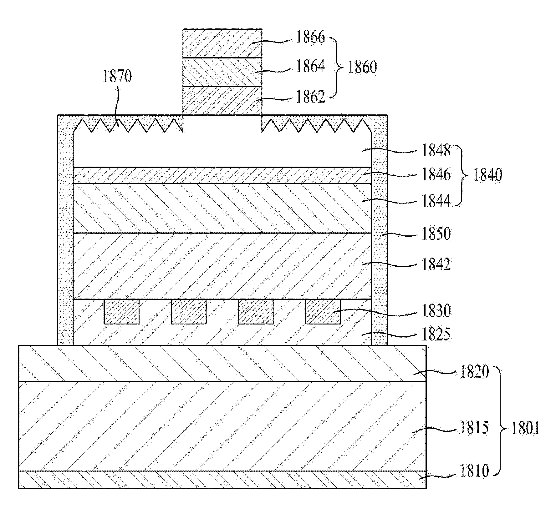
[0268 represents a measured temperature of the light emitting chip when a length of the first direction of the first portion and the second portion in the side surface part of the first lead frame is identical to that of the third portion. Case 2 represents a measured temperature of the light emitting chip illustrated in FIG. 22. Case 3 represents a measured temperature of the light emitting chip illustrated in FIG. 33.

[0269]Referring to FIG. 40, the measured temperature (t1) of case 1 is 44.54° C., the measured temperature (t2) of case 2 is 43.66° C., and the measured temperature (t3) of case 3 is 43.58° C.

[0270]Accordingly, as designs of the connection parts of the first side surface part 714 of the first lead frame 620 are changed, a heat dissipation effect of the present exemplary embodiment can be improved. Thus, since an increase in temperature of the light emitting chip 640 mounted to the light emitting device packages 200-1, 200-2 at the time of light emission may be relieve...


PUM


Abstract

Provided is a lighting device, comprising: a light source module comprising: at least one light source disposed on a printed circuit board; and a resin layer disposed on the printed circuit board so that the light source is embedded; a light reflection member formed on at least any one of one side surface and another side surface of the resin layer; and a diffusion plate having an upper surface formed on the light source module, and a side wall which is integrally formed with the upper surface and formed to extend in a lower side direction and which is adhered onto the light reflection member, wherein a first separated space is formed between the light source module and the upper surface of the diffusion plate, whereby flexibility of the product itself can be secured, and durability and reliability of the product can be also improved.

Description

CROSS-REFERENCE TO RELATED APPLICATIONS[0001]This application claims the benefit under 35 U.S.C. §119 of Korean Patent Application Nos. 10-2012-0065259, filed Jun. 18, 2012; 10-2012-0065260, filed Jun. 18, 2012; and 10-2012-0065264, filed Jun. 18, 2012, which are hereby incorporated by reference in their entirety.BACKGROUND[0002]1. Field of the Invention[0003]Embodiments of the present invention relate to the technology field of a lighting device.[0004]2. Description of the Related Arts[0005]An LED (Light Emitted Diode) device is a device which converts an electrical signal to infrared rays or light using a composition semiconductor property. Unlike a florescent lamp, since the LEI) device does not use harmful substances such as mercury and the like, it has a low possibility to cause environmental pollution and a long life span compared to a conventional light source. Also, it is advantageous that the LED device spends low electricity compared to the conventional light source and ha...

Claims


Application Information

Patent Timeline
Patent Type & Authority Applications(United States)
IPC IPC(8): F21V13/02
CPCF21V13/02F21V3/02F21V3/04F21V15/012F21V31/04H01L2224/48091H01L2224/48247F21Y2105/10F21Y2115/10F21S43/15F21S43/14F21S43/195F21S41/30F21S43/20F21S43/30F21S41/192F21S41/20F21V13/08H01L2924/00014H01L25/0753H01L33/48B60Q1/30G02B6/0031G02B6/0051G02B6/0055G02B6/0083G02B6/0085G02B6/0088G02B6/0095H01L33/62F21V29/503F21V29/70B60Q1/0011B60Q1/04B60Q1/2696H01L33/56H01L33/58H01L33/60F21S41/663F21S41/32
Inventor PARK, KWANG HOKIM, CHUL HONGYANG, HYUN DUCKPARK, MOO RYONGHYUN, JUN CHUL
Owner LG INNOTEK CO LTD
Why Eureka
Try Eureka