A kind of oled array substrate, display panel and display device

A technology of array substrates and sub-pixels, which is applied to instruments, semiconductor devices, computing, etc., and can solve problems affecting display effects, etc.

Active Publication Date: 2019-03-29
SHANGHAI TIANMA MICRO ELECTRONICS CO LTD +1
View PDF3 Cites 0 Cited by
  • Summary
  • Abstract
  • Description
  • Claims
  • Application Information

AI Technical Summary

Problems solved by technology

[0006] In view of this, the present invention provides an OLED array substrate, a display panel, and a display device to solve the problem in the prior art that the resistive pressure-sensitive element is placed in the display area of ​​the OLED panel and affects the display effect.

Method used


Image

  • A kind of oled array substrate, display panel and display device
  • A kind of oled array substrate, display panel and display device
  • A kind of oled array substrate, display panel and display device

Examples


Embodiment Construction

[0028] The following will clearly and completely describe the technical solutions in the embodiments of the present invention with reference to the accompanying drawings in the embodiments of the present invention. Obviously, the described embodiments are only some, not all, embodiments of the present invention. Based on the embodiments of the present invention, all other embodiments obtained by persons of ordinary skill in the art without making creative efforts belong to the protection scope of the present invention.

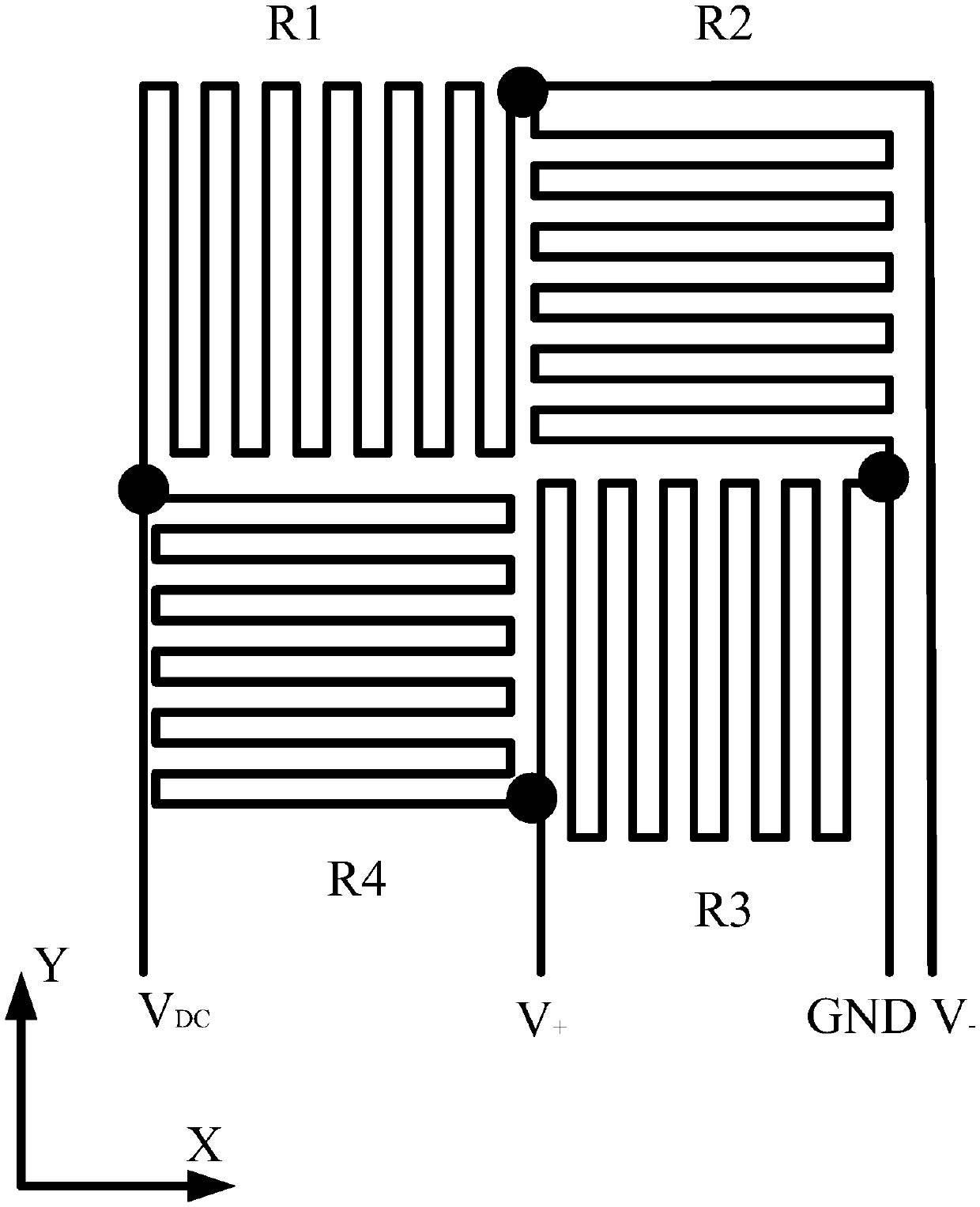
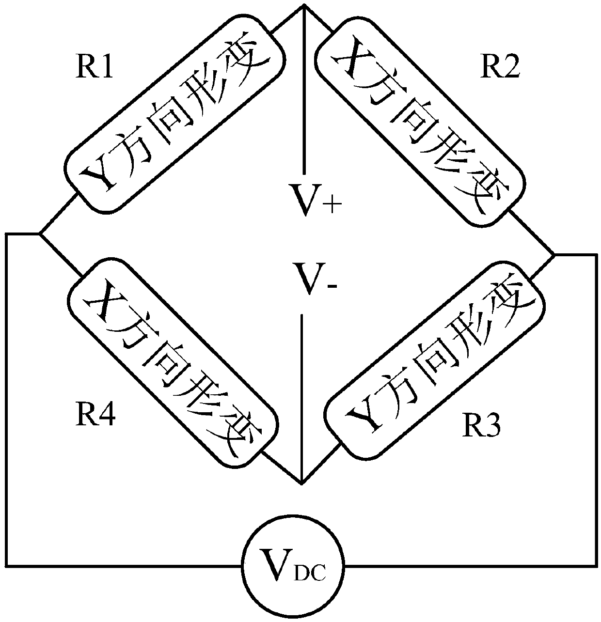
[0029] The touch display panel in the prior art usually has a rectangular structure and includes a display area and a black frame area surrounding the display area. figure 1 The resistive pressure-sensing element shown is fabricated in the frame area. When the display panel is pressed and deformed, the strain difference in the two orthogonal directions of the X direction and the Y direction is used to read the change of the voltage signal, thereby realizing pre...


PUM


Abstract

The present application provides an OLED array substrate including a plurality of sub-pixels defined by a plurality of data lines and a plurality of scanning lines, and a resistive pressure-sensitive element located in the non-opening area of ​​the plurality of sub-pixels. The resistive pressure-sensitive element is composed of a plurality of Composed of resistors, multiple resistors are in a serpentine wiring structure. The serpentine wiring structure includes a first sub-wiring and a second sub-wiring connecting two adjacent first sub-wirings. The first sub-wiring and the second sub-wiring The two sub-wires are located in the non-opening areas of multiple sub-pixels of the OLED array substrate, so that the resistive pressure-sensitive element is fabricated in the display area of ​​the OLED array substrate without affecting the display effect of the display panel or display device. In addition, the extending direction of the projection of the first sub-wire on the array substrate intersects the extending direction of the projection of the plurality of data lines and the plurality of scanning lines on the array substrate, so that the resistive pressure-sensitive element can obtain better pressure. Sensitive signal, improve the performance of pressure sensing detection.

Description

technical field [0001] The present invention relates to the field of display technology, in particular to an OLED (Organic Light Emitting Diode, Organic Light Emitting Diode) array substrate, a display panel and a display device. Background technique [0002] Pressure-sensing technology is to add a pressure-sensing device to the screen of the mobile phone. Touching the screen with a finger and pressing it hard will bring different interactive effects. That is to say, the screen can sense different strengths such as light touch, normal touch and heavy pressure, so that the finger operation can be felt more three-dimensionally, and more diverse operation modes can be realized. The first appearance of pressure sensing is the pressure touch technology proposed by Apple, which has been widely used in the market. [0003] OLED display panels in the prior art use resistive pressure-sensitive elements to realize pressure sensing, such as figure 1 and figure 2 as shown, figure 1...

Claims


Application Information

Patent Timeline
Patent Type & Authority Patents(China)
IPC IPC(8): G06F3/041
CPCG06F3/0412G06F3/0414H10K59/82H10K59/12G06F3/0416G06F3/04144G06F2203/04105G06F3/045G06F2203/04111H10K59/00H10K59/40H10K59/131H10K59/351
Inventor 曾洋周星耀王丽花刘亮
Owner SHANGHAI TIANMA MICRO ELECTRONICS CO LTD
Why Eureka
Try Eureka