Ball grid array printed circuit board

A printed circuit board and ball grid array technology applied in the electronic field to achieve the effects of improving portability, improving component integration, and increasing effective wiring area

Inactive Publication Date: 2017-05-10
NUBIA TECHNOLOGY CO LTD
View PDF5 Cites 2 Cited by
  • Summary
  • Abstract
  • Description
  • Claims
  • Application Information

AI Technical Summary

Problems solved by technology

[0003] The technical problem to be solved by the present invention is: in the existing ball grid array printed circuit board, only the pads at the edge of the array can go out on the surface of the circuit board, while the pads in the middle of the array need to open holes on the circuit board. Through openings, the pads in the middle of the array are electrically connected to the wiring layers in the middle of the circuit board or the circuits on the wiring layer on the back of the circuit board, so that there are more openings, which reduces the effective wiring area of ​​the circuit board. It is not conducive to improving the component integration of the circuit board; and in the case of deploying the same number of electronic components, the more holes are punched, the larger the volume of the circuit board, which is not conducive to improving the portability of electronic equipment, thereby reducing the use of Satisfaction with electronic equipment

Method used


Image

  • Ball grid array printed circuit board
  • Ball grid array printed circuit board
  • Ball grid array printed circuit board

Examples


no. 1 example

[0024] In order to reduce the number of openings on the ball grid array printed circuit board, increase the effective wiring area of ​​the circuit board, improve the integration of circuit board components, reduce the volume of the circuit board, improve the portability of electronic equipment, and improve the use of electronic equipment by users. Equipment satisfaction, this embodiment provides a new ball grid array printed circuit board.

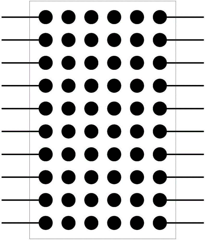
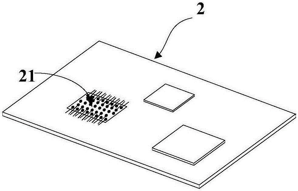
[0025] refer to figure 2 , figure 2 It is a schematic diagram of the structure of the BGA printed circuit board provided by the first embodiment of the present invention. The BGA printed circuit board 2 includes a first pad array 21 . Wherein, the structure of the first pad array 21 can be referred to image 3 , including n pad queues (n≥2), each pad queue is recorded as the first pad queue, the second pad queue, ..., the nth pad queue according to the order from near to far from the outlet side .

[0026] It should be understood tha...

no. 2 example

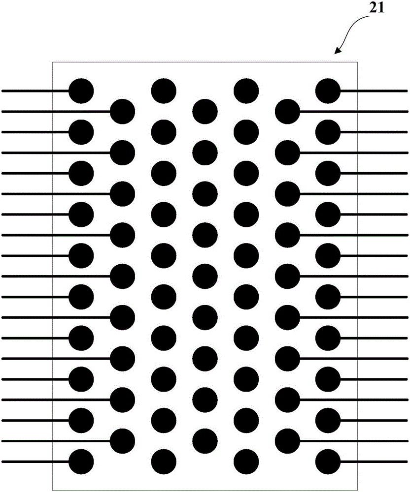
[0044] In this embodiment, on the basis of the first embodiment, the present invention will be further described by taking the way that each third pad in the third pad array goes out on the surface of the BGA printed circuit board as an example.

[0045] refer to Figure 6 , Figure 6 A schematic diagram of the structure of a first pad array provided by the second embodiment of the present invention, wherein each pad in the second pad array is alternately arranged with each first pad in the first pad array, and the third pad The third pads in the pad alignment are alternately arranged with the second pads in the second pad alignment. When going out, the third pad comes out from between the two adjacent second pads, and is parallel to the outgoing line of one of the second pads, and connects from the two first pads adjacent to the second pad. pass between plates.

[0046] It is worth noting that when going out, the distance between two adjacent second pads should be greater ...


PUM


Abstract

The invention discloses a ball grid array printed circuit board, which is provided with a first pad array comprising at least two pad queues. Various first pads in the first pad queue adjacent to an outlet side of the first pad array are interleaved with various second pads in the second pad queue adjacent to the first pad queue and far away from the outlet side, and the spacing between two adjacent first pads is set to be equal to or greater than 3 times the outlet wire width of each second pad, so that each second pad outputs a wire from between the two first pads adjacent thereto. In this way, the number of pads that output a wire on the surface of the ball grid array printed circuit board is increased, the number of openings on the circuit board is reduced, the effective wiring area of the circuit board is increased, the component integration degree of the circuit board is increased, the size of the circuit board is reduced to a certain extent, the portability of electronic equipment is improved, and thus, the user's satisfaction with the use of the electronic equipment is improved.

Description

technical field [0001] The invention relates to the field of electronic technology, more specifically, to a ball grid array printed circuit board. Background technique [0002] With the continuous development of electronic technology, electronic components are becoming more and more miniaturized and integrated. For this, people use a ball grid array packaging technology to package surface mount components on circuit boards. The currently used ball grid array printed circuit board, its pad array structure can be found in figure 1 , only the pads on the edge of the array can go out on the surface of the circuit board, while the pads in the middle of the array need to open holes on the circuit board, through which the pads in the middle of the array are connected to the wiring layers in the middle of the circuit board Or the circuits on the wiring layer on the back of the circuit board are electrically connected. However, the openings on the circuit board will destroy the str...

Claims


Application Information

Patent Timeline
Patent Type & Authority Applications(China)
IPC IPC(8): H05K1/02H05K1/11
CPCH05K1/02H05K1/11
Inventor 陈望虹王芳李建发
Owner NUBIA TECHNOLOGY CO LTD
Why Eureka
Try Eureka