Display module, binding detection system and binding system

A display module and bonding technology, applied in semiconductor/solid-state device testing/measurement, electrical components, electrical solid-state devices, etc., which can solve problems such as mechanical errors, waste of bonding materials, and offset of bonding positions

Active Publication Date: 2017-05-31
BOE TECH GRP CO LTD +1
View PDF6 Cites 18 Cited by
  • Summary
  • Abstract
  • Description
  • Claims
  • Application Information

AI Technical Summary

Problems solved by technology

[0004] However, due to mechanical errors in the binding process or expansion caused by the expiration of the material itself, the actual binding position is offset
In the same batch of bonding process, several display devices after bonding will be randomly selected at the beginning of the whole batch, and the offset after bonding will be measured manually with a microscope, which will consume a lot of time and manpower, making the binding efficiency low; and, because the material expansion problem can only be found through an artificial microscope, it will cause a great waste of binding materials

Method used


Image

  • Display module, binding detection system and binding system
  • Display module, binding detection system and binding system
  • Display module, binding detection system and binding system

Examples


Embodiment Construction

[0029] The following will clearly and completely describe the technical solutions in the embodiments of the present invention with reference to the accompanying drawings in the embodiments of the present invention. Obviously, the described embodiments are only some, not all, embodiments of the present invention. Based on the embodiments of the present invention, all other embodiments obtained by persons of ordinary skill in the art without making creative efforts belong to the protection scope of the present invention.

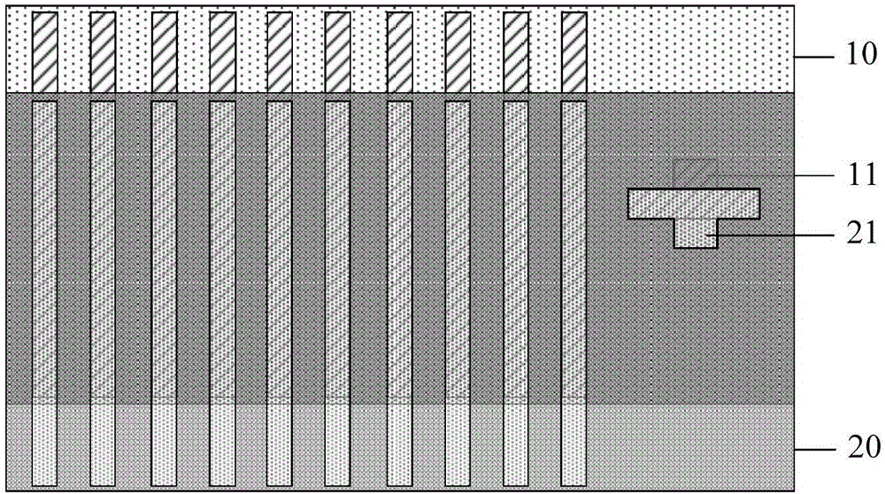
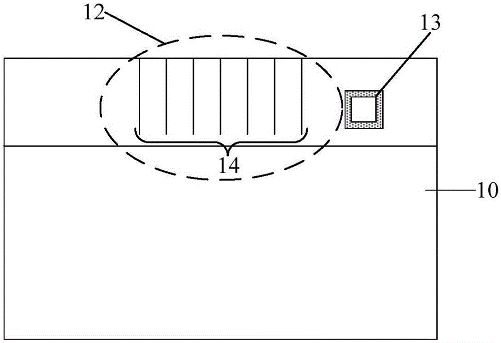
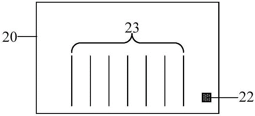
[0030] An embodiment of the present invention provides a display module, such as Figure 2-4 As shown, the display panel 10 and COF20 are included, and the COF20 is bound in the binding area 12 of the display panel 10; the display panel 10 also includes a first alignment mark 13, along the direction of the side of the display panel 10 close to the binding area 12, the second A pair of alignment marks 13 are arranged on at least one side of the binding area 12;...


PUM


Abstract

The invention provides a display module, a binding detection system and a binding system and relates to the technical field of display. Whether a COF is qualified or not can be automatically detected, so that the waste of a binding material is reduced and the binding efficiency is improved. The display module comprises a display panel and the COF, wherein the COF is bound to a binding area of the display panel; the display panel also comprises first alignment identifiers; the first alignment identifiers are arranged on at least one side of the binding area along the direction, close to the edge of the display panel, of the binding area; the COF also comprises second alignment identifiers; the second alignment identifiers are in one-to-one correspondence with the first alignment identifiers; the second alignment identifiers are used for being aligned at the first alignment identifiers, wherein the first alignment identifiers are of a hollow structure; the second alignment identifiers are of a solid structure; and the second alignment identifiers can be embedded into the hollow parts of the first alignment identifiers.

Description

technical field [0001] The invention relates to the field of display technology, in particular to a display module, a binding detection method and a binding system. Background technique [0002] COF (Chip On Film, Chip On Film) is a chip soft film construction technology that fixes IC (Intergrated Circuit) on a flexible circuit board. The COF is usually bound in the binding area of ​​the display panel to drive the display device. During this process, the COF needs to be precisely aligned with the display panel. [0003] Currently, if figure 1 As shown, an upper half cross pattern 11 and a lower half cross pattern 21 are respectively arranged on the display panel 10 and a lower half cross pattern 21, wherein, the upper half cross pattern 11 and the lower half cross pattern 21 are upright, and the other is upside down, and the binding ( When the Bonding process is aligned, the horizontal strip portion of the upper half cross pattern 11 of the display panel 10 is overlapped w...

Claims


Application Information

Patent Timeline
Patent Type & Authority Applications(China)
IPC IPC(8): H01L21/66H01L21/67H01L21/603H01L23/544
CPCH01L21/67259H01L22/20H01L23/544H01L24/75H01L2223/54426H01L2224/75754H01L2224/759Y02P80/30
Inventor 蔡振飞徐攀李永谦曹昆程雪连程荣梅
Owner BOE TECH GRP CO LTD
Why Eureka
Try Eureka