Method of making near chip size integrated circuit package

a technology of integrated circuits and chips, applied in the field of electronic packaging, can solve the problems of reducing the weight and size of electronic devices, affecting the reworking of assembly, so as to reduce the cost and weight of the package, avoid delamination and thermal cracking

Inactive Publication Date: 2005-11-08
AMKOR TECH SINGAPORE HLDG PTE LTD
View PDF67 Cites 149 Cited by
  • Summary
  • Abstract
  • Description
  • Claims
  • Application Information

AI Technical Summary

Benefits of technology

[0016]The encapsulant layer electrically isolates the shield layer from the IC chip and the various electrical conductors (e.g. bonding pads, bond wires, contacts and metallizations). The shield layer, being an electrically conductive material, forms a floating ground plane which shields the IC chip and the remainder of the package. Thus, the shield layer prevents external radiation form interfering with the operation of the package

Problems solved by technology

However, metal shielding is relatively expensive and inhibits reduction in weight and size of electronic devices.
However, applying the electrically insulating/conductive layers after the semiconductor devices are attached to the printed circuit board adds complexity to the manufacturing process and hinders re

Method used


Image

  • Method of making near chip size integrated circuit package
  • Method of making near chip size integrated circuit package
  • Method of making near chip size integrated circuit package

Examples


Embodiment Construction

[0040]In accordance with the present invention, a near chip size integrated circuit package, called a CHIPARRAY™ package, is presented.

[0041]Several elements shown in the following figures are substantially similar. Therefore, similar reference numbers are used to represent similar elements.

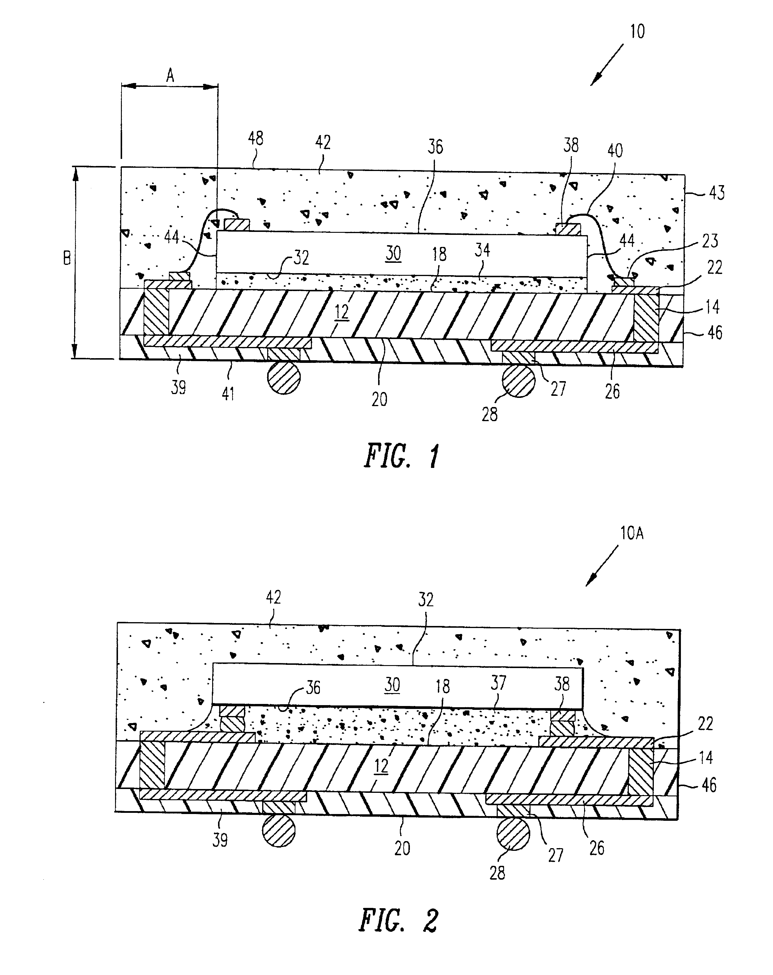
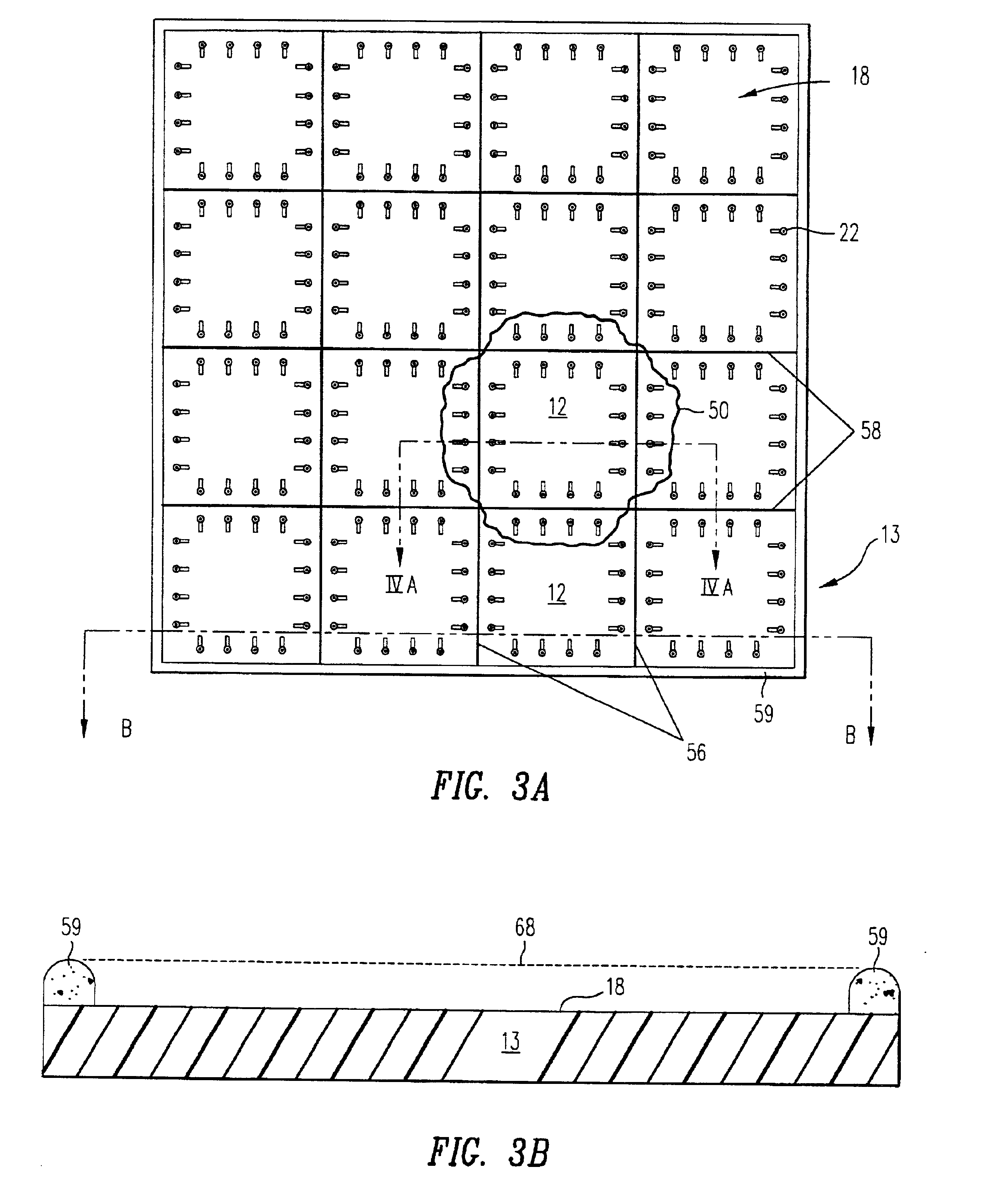
[0042]FIG. 1 is a cross-sectional view of a package 10 in accordance with one embodiment of the present invention. Package 10 includes an insulating substrate 12 having electrically conductive through-holes 14.

[0043]For example, by drilling holes in substrate 12 and then plating the drilled holes with a conductive material such as copper, conductive through-holes 14 are formed. Illustratively, copper is plated to a minimum thickness of 600 micro inches (μ in).

[0044]Substrate 12 is typically a ceramic, a laminate, a passivated metal or a printed circuit board substrate material. Examples of suitable ceramic substrates include 98% alumina or 98% aluminum nitride ceramic substrates available from Su...


PUM

PropertyMeasurementUnit
Lengthaaaaaaaaaa
Lengthaaaaaaaaaa
Lengthaaaaaaaaaa

Abstract

A plurality of integrated circuit chip (IC chip) packages are fabricated simultaneously from a single insulating substrate having sections. In each section, an IC chip is attached. Bonding pads on the IC chip are electrically connected to first metallizations on a substrate first surface. The first metallizations, IC chip including bonding pads and first substrate surface are then encapsulated. Interconnection balls or pads are formed at substrate bonding locations on a substrate second surface, the interconnection pads or balls being electrically connected to corresponding first metallizations. The substrate and encapsulant are then cut along the periphery of each section to form the plurality of IC chip packages.

Description

CROSS-REFERENCE TO RELATED APPLICATIONS[0001]This application is a division of U.S. patent application Ser. No. 09 / 585,901, filed Jun. 2, 2000, now abandoned, which is a division of U.S. patent application Ser. No. 09 / 083,524, filed May 22, 1998, now U.S. Pat. No. 6,150,193, which is continuation-in-part of U.S. patent application Ser. No. 08 / 741,797, filed Oct. 31, 1996, now U.S. Pat. 5,981,314, by Thomas P. Glenn et al., all of which applications are herein incorporated by reference in their respective entirety.FIELD OF THE INVENTION[0002]The present invention relates to the art of electronic packaging and more particularly to a method of packaging an integrated circuit chip and the resulting structure.BACKGROUND OF THE INVENTION[0003]As electronic devices become increasingly compact and lightweight, it becomes increasingly desirable to reduce the size of integrated circuit chip (IC chip) packages. In addition to reducing the size of IC chip packages, it is also desirable to simul...

Claims


Application Information

Patent Timeline
IPC IPC(8): H01L21/56H01L21/02H01L23/31H01L23/28H01L23/552
CPCH01L21/56H01L21/561H01L23/3128H01L23/552H01L24/97H01L24/45H01L2224/16225H01L2224/32225H01L2224/45124H01L2224/45144H01L2224/48091H01L2224/48227H01L2224/73204H01L2224/73265H01L2224/97H01L2924/01013H01L2924/01015H01L2924/01029H01L2924/0105H01L2924/01078H01L2924/01079H01L2924/01082H01L2924/01322H01L2924/14H01L2924/15184H01L2924/15311H01L2924/3025H01L24/48H01L2924/01005H01L2924/01006H01L2924/01019H01L2924/01033H01L2924/01087H01L2924/1815H01L2924/01028Y10T29/49135H01L2924/00014H01L2224/85H01L2224/83H01L2224/92247H01L2224/81H01L2924/00012H01L2924/00H01L2924/12042H01L24/73H01L2224/05573H01L2224/05568H01L2924/181H01L2924/15183H01L2224/06135H01L2224/05599
Inventor GLENN, THOMAS P.HOLLAWAY, ROY D.PANCZAK, ANTHONY E.
Owner AMKOR TECH SINGAPORE HLDG PTE LTD
Why Eureka
Try Eureka