Manufacturing method of liquid crystal display panel with narrow bezel

The technology of a liquid crystal display panel and a manufacturing method is applied in the directions of nonlinear optics, instruments, optics, etc., and can solve the problems of large occupied space, large size of the liquid crystal display panel 203, unfavorable narrow frame of the liquid crystal display panel 203, etc., and achieve reduction Frame size, to achieve the effect of narrow frame

Inactive Publication Date: 2017-06-09
WUHAN CHINA STAR OPTOELECTRONICS TECH CO LTD
View PDF3 Cites 13 Cited by
  • Summary
  • Abstract
  • Description
  • Claims
  • Application Information

AI Technical Summary

Problems solved by technology

The manufacture method of existing liquid crystal display panel comprises the steps: step 1, such as figure 1 As shown, a liquid crystal display motherboard 1 is provided, and a plurality of panel units 2 arranged in an array are fabricated on the liquid crystal display motherboard 1; each panel unit 2 includes a display area (Active Area, AA) 201, and a plurality of test points 202 located above the display area 201 and electrically connected to the display area 201; step 2, such as figure 2 As shown, the liquid crystal display motherboard 1 is cut along two adjacent columns of

Method used


Image

  • Manufacturing method of liquid crystal display panel with narrow bezel
  • Manufacturing method of liquid crystal display panel with narrow bezel
  • Manufacturing method of liquid crystal display panel with narrow bezel

Examples


Embodiment Construction

[0031] In order to further illustrate the technical means adopted by the present invention and its effects, the following describes in detail in conjunction with preferred embodiments of the present invention and accompanying drawings.

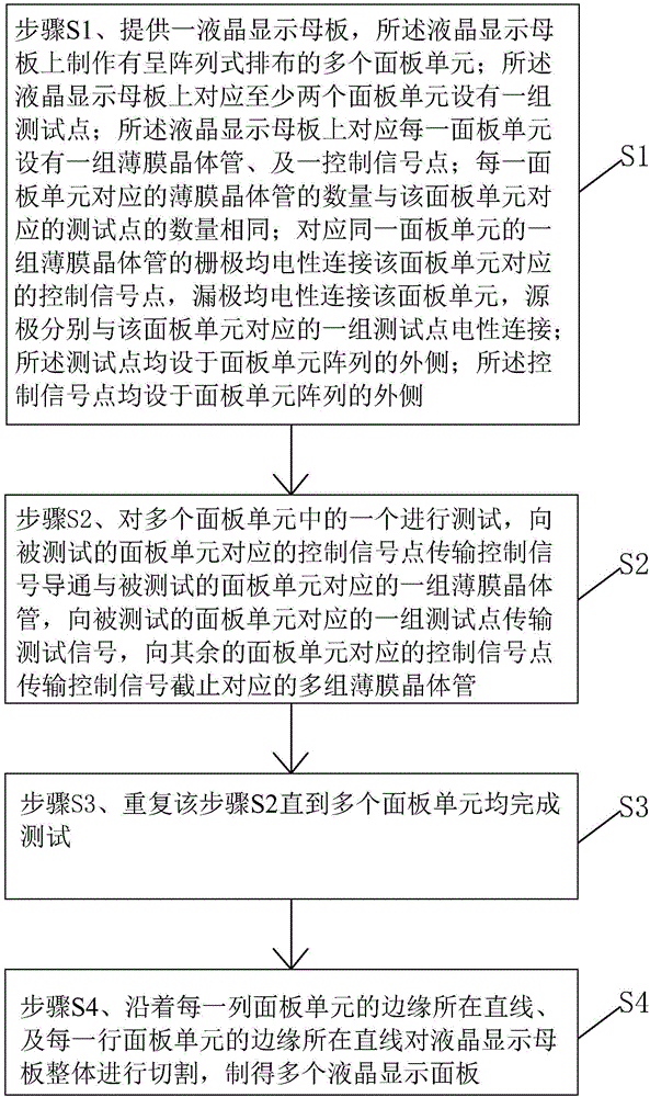
[0032] see image 3 , the invention provides a method for manufacturing a narrow-frame liquid crystal display panel, comprising the following steps:

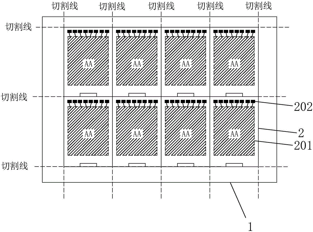
[0033] Step S1, please refer to Figure 4 , providing a liquid crystal display motherboard 10, the liquid crystal display motherboard 10 is fabricated with a plurality of panel units 20 arranged in an array;

[0034] A set of test points 11 are provided on the LCD motherboard 10 corresponding to at least two panel units 20;

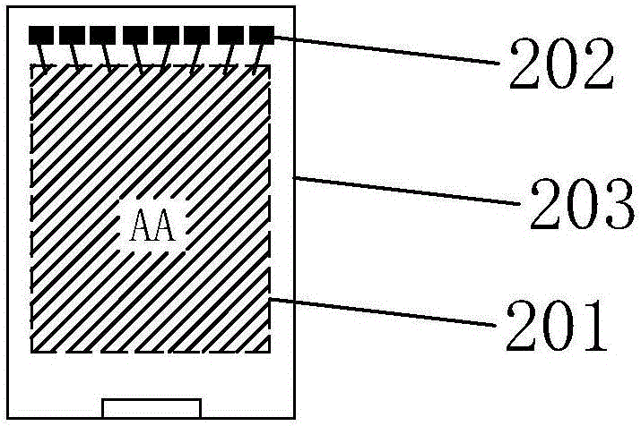
[0035] A group of thin film transistors 22 and a control signal point 12 are arranged corresponding to each panel unit 20 on the liquid crystal display motherboard 10; the same number of

[0036] The gates of a group of thin film transistors 22 corresponding to the same...


PUM


Abstract

The invention provides a manufacturing method of a liquid crystal display panel with a narrow bezel. A plurality of panel units arranged in an array mode are manufactured on the liquid crystal display master panel, a group of testing points are arranged corresponding to the panel units, a group of thin film transistors and a control signal point are arranged corresponding to each panel unit, and the testing points and the control signal points are all arranged on the outer side of the panel unit array. When panel unit testing is conducted, one corresponding group of thin film transistors are controlled to be connected by transmitting a control signal to the control signal point corresponding to a to-be-tested panel unit, a testing signal is transmitted to one corresponding group of testing points, control signals are transmitted to the other control signal points to control the corresponding groups of thin film transistors to be cut off so that it can be ensured that each panel unit can be tested independently, the bezel size of the liquid crystal display panel manufactured after a cutting process is reduced, and the narrow bezel of the liquid crystal display panel is easily achieved.

Description

technical field [0001] The invention relates to the field of display technology, in particular to a method for manufacturing a liquid crystal display panel with a narrow frame. Background technique [0002] With the development of display technology, liquid crystal displays (Liquid Crystal Display, LCD) and other flat display devices are widely used in mobile phones, televisions, personal Various consumer electronic products such as digital assistants, digital cameras, notebook computers, and desktop computers have become the mainstream of display devices. [0003] Most of the liquid crystal display devices currently on the market are backlight liquid crystal displays, which include a liquid crystal display panel and a backlight module (Backlight Module). The working principle of the liquid crystal display panel is to place liquid crystal molecules between two parallel glass substrates. There are many vertical and horizontal small wires between the two glass substrates. The...

Claims


Application Information

Patent Timeline
IPC IPC(8): G02F1/1333G02F1/1362
CPCG02F1/133351G02F1/1362G02F1/136254
Inventor 洪光辉龚强陈归
Owner WUHAN CHINA STAR OPTOELECTRONICS TECH CO LTD
Why Eureka
Try Eureka