
Pixel circuit and driving method thereof, display panel and display device

A pixel circuit and electrode technology, applied in the field of flat display, can solve the problems of screen display jitter, unevenness, current and voltage difficulties, etc., and achieve the effect of achieving brightness

Active Publication Date: 2019-02-22
KUNSHAN GO VISIONOX OPTO ELECTRONICS CO LTD
View PDF6 Cites 0 Cited by
  • Summary
  • Abstract
  • Description
  • Claims
  • Application Information

AI Technical Summary

Problems solved by technology

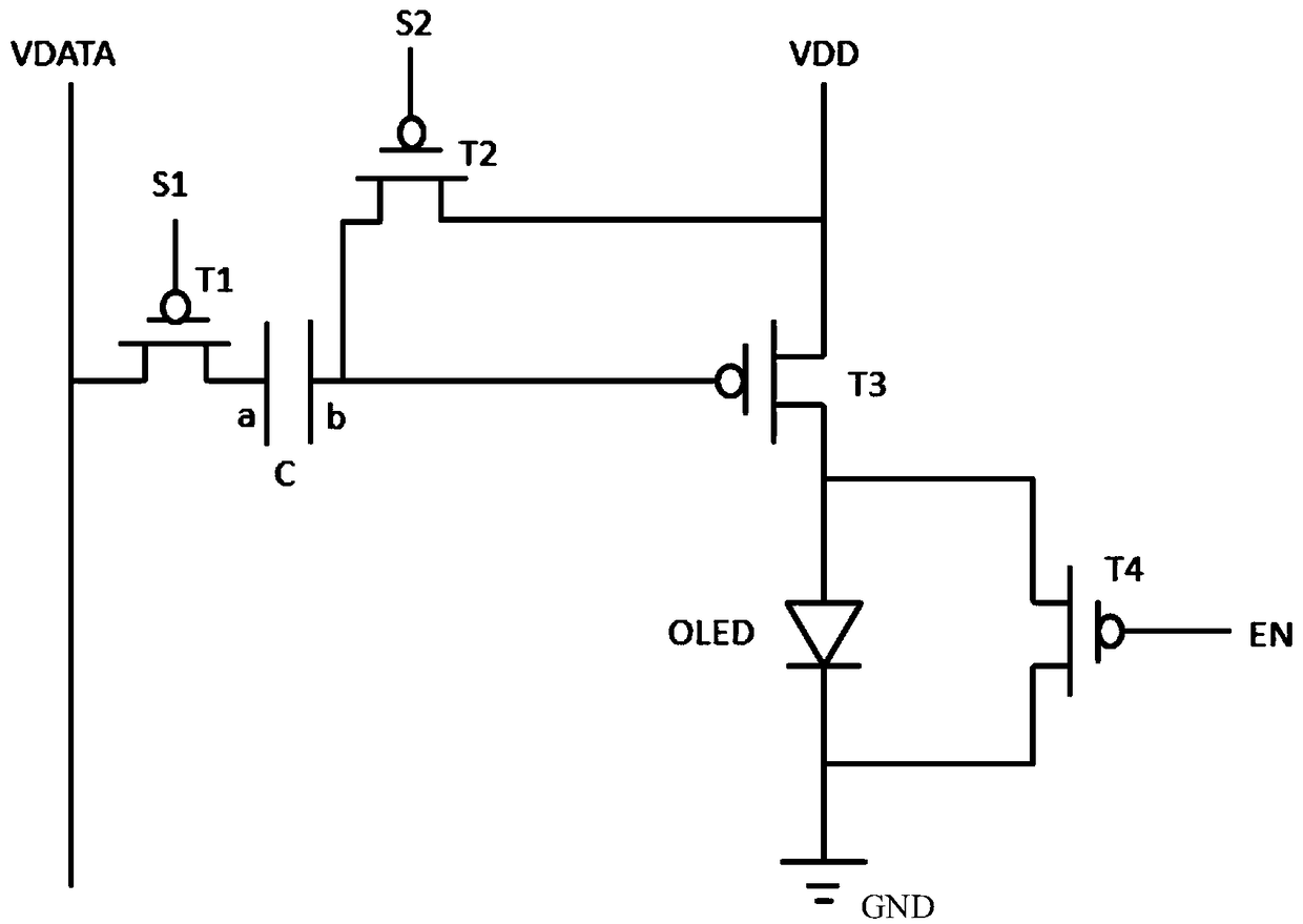
[0003] In the field of OLED lighting, the OLED display brightness is mainly controlled by controlling the current flowing through the OLED or the voltage across the OLED. However, due to the influence of other interference factors such as noise, it is difficult to achieve accurate control of the current and voltage, which will cause the screen Display jitter, unevenness, etc.

Method used


Image

  • Pixel circuit and driving method thereof, display panel and display device
  • Pixel circuit and driving method thereof, display panel and display device

Examples


Embodiment Construction

[0031] In order to make the content of the present invention clearer and easier to understand, the content of the present invention will be further described below in conjunction with the accompanying drawings. Of course, the present invention is not limited to this specific embodiment, and general replacements known to those skilled in the art are also covered within the protection scope of the present invention.

[0032] Secondly, the present invention is described in detail using schematic diagrams. When describing the embodiments of the present invention in detail, for convenience of explanation, the schematic diagrams are not partially enlarged according to the general scale, which should not be used as a limitation of the present invention.

[0033] One of the core ideas of the present invention is that the present invention provides a pixel circuit, including: a first transistor, a second transistor, a third transistor, a capacitor, and a light emitting diode, wherein th...


PUM


Abstract

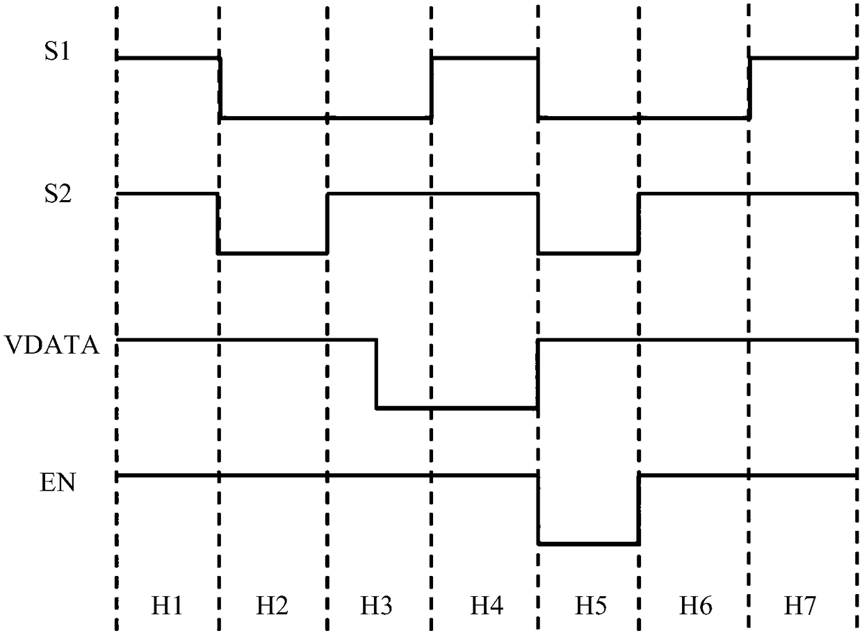
The invention provides a pixel circuit and a driving method thereof, a display panel and a display device. The pixel circuit comprises three transistors, one capacitor and one organic light emitting diode (OLED), wherein the grid of a first transistor is connected with a first control signal, the first electrode is connected with a data signal, and the second electrode is connected with one end of the capacitor; the grid of the second transistor is connected with a second control signal, the first electrode is connected with the other end of the capacitor, and the second electrode is connected with a power supply voltage signal; the grid of a third transistor is connected with one end of the capacitor, the first electrode is connected with the organic light emitting diode, and the second electrode is connected with the power supply voltage signal; turn-on time and turn-off time of the first transistor and the second transistor are controlled by virtue of time sequences of the first control signal and the second control signal, so that voltage values of the two ends of the capacitor are controlled; and turn-on time of the third transistor is controlled by virtue of changes of the voltage values, so that duty ratio of lightening time of the OLED in one period is adjusted, and accurate control on brightness of the OLED is realized.

Description

technical field [0001] The present invention relates to the technical field of plane display, in particular to a pixel circuit and its driving method, a display panel and a display device. Background technique [0002] Organic light-emitting devices, that is, Organic Light-Emitting Diode (OLED for short), also known as Organic Electroluminescence Display (OLED for short), have wide viewing angles, high brightness, high contrast, low energy consumption, and smaller volumes. Advantages such as lightness and thinness are the focus of attention of flat panel display technology at present. [0003] In the field of OLED lighting, the OLED display brightness is mainly controlled by controlling the current flowing through the OLED or the voltage across the OLED. However, due to the influence of other interference factors such as noise, it is difficult to achieve accurate control of the current and voltage, which will cause the screen Shows issues with jitter, unevenness, etc. [0...

Claims


Application Information

Patent Timeline
Patent Type & Authority Patents(China)
IPC IPC(8): G09G3/3258G09G3/3266
CPCG09G3/3258G09G3/3266G09G2320/0233
Inventor 张春雷
Owner KUNSHAN GO VISIONOX OPTO ELECTRONICS CO LTD
Learn More