Check patentability & draft patents in minutes with Patsnap Eureka AI!

Array substrate, manufacturing method thereof, display panel and display device

A technology for array substrates and substrate substrates, applied in optics, instruments, electrical digital data processing, etc., can solve problems such as reducing the penetration rate of liquid crystal display devices, and achieve the effect of reducing the number and increasing the penetration rate

Pending Publication Date: 2017-06-16
XIAMEN TIANMA MICRO ELECTRONICS
View PDF4 Cites 3 Cited by
  • Summary
  • Abstract
  • Description
  • Claims
  • Application Information

AI Technical Summary

Problems solved by technology

[0004] The transmittance of the liquid crystal display device is affected by the transmittance of the array substrate, the transmittance of the color filter substrate, etc. Due to the increase of the insulating layer and the limitation of the refractive index of the insulating layer material, the overall transmittance of the liquid crystal display device is reduced. rate problem

Method used


Image

  • Array substrate, manufacturing method thereof, display panel and display device
  • Array substrate, manufacturing method thereof, display panel and display device
  • Array substrate, manufacturing method thereof, display panel and display device

Examples


Embodiment

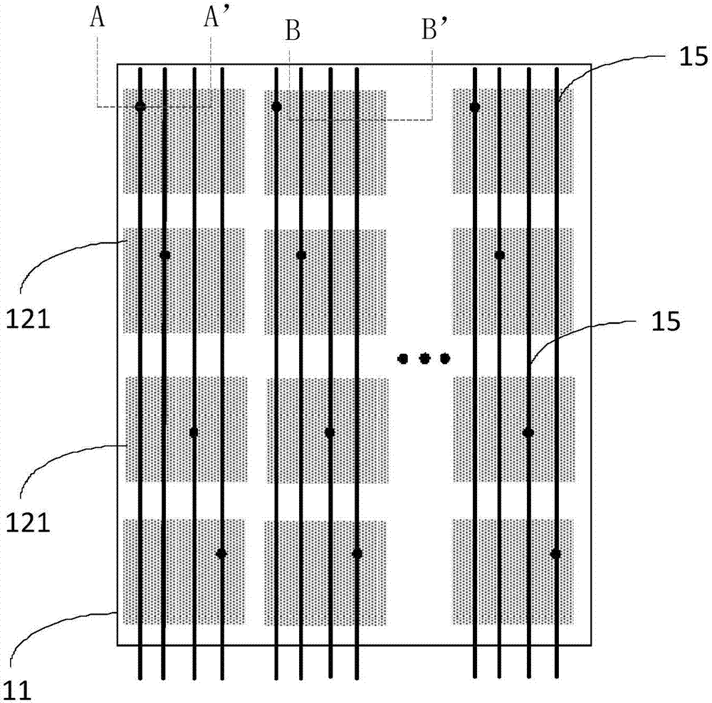
[0051] figure 1 The first plan view of the array substrate provided by the embodiment of the present invention, figure 2 for figure 1 Schematic diagram of the cross-sectional structure along AA' in the middle, image 3 for figure 1 Schematic diagram of the cross-sectional structure along BB' in the center, such as figure 1 , figure 2 and image 3 As shown, the array substrate provided by the embodiment of the present invention includes a base substrate 11 , a common electrode layer 12 , a first insulating layer 13 , a pixel electrode 14 , and a touch signal line 15 .

[0052]In addition, a buffer layer 21 is provided between the base substrate 11 and the common electrode layer 12, a gate insulating layer 22 is provided on the side of the buffer layer 21 away from the base substrate 11, and a gate insulating layer 22 is provided on the side far away from the base substrate. 11 is provided with a data line insulating layer 23, a data line 16 is provided on the side of th...


PUM

PropertyMeasurementUnit
Thicknessaaaaaaaaaa

Abstract

The embodiment of the invention discloses an array substrate, a manufacturing method thereof, a display panel and a display device. The array substrate comprises a substrate base plate, a common electrode layer, a first insulating layer, a pixel electrode located on the side deviating from the substrate base plate, of the first insulating layer, and touch signal lines located on the side deviating from the substrate base plate, of the first insulating layer, wherein the common electrode layer comprises multiple common electrode units, the common electrode units are reused as touch electrodes at a touch stage, the first insulating layer is located on the side, deviating from the substrate base plate, of the common electrode layer, each common electrode unit and at least one touch signal line are connected through via holes formed in the first insulating layer, and the touch signal lines and the pixel electrode are arranged in an insulated mode. By adopting the technical scheme, adjustment of a film layer structure of the array substrate in the prior art is achieved, the number of insulation layers is decreased, and accordingly the effect of improving the penetration rate is achieved.

Description

technical field [0001] The present invention relates to the technical field of touch display, in particular to an array substrate and a manufacturing method thereof, a display panel and a display device. Background technique [0002] In a liquid crystal display device, a panel with a touch function is used in order to allow a user to perform related operations while watching a screen. In the prior art, the touch function is realized by adding a layer of touch electrode layer on the basis of the display panel or integrating the touch electrode layer inside the display panel. [0003] In the method of integrating the touch electrode layer inside the display panel, not only the touch electrode layer but also an insulating layer must be added inside the display panel, so that the touch electrode layer can be insulated from other conductive layers. [0004] The transmittance of the liquid crystal display device is affected by the transmittance of the array substrate, the transmi...

Claims


Application Information

Patent Timeline
IPC IPC(8): G02F1/1362G02F1/1333G06F3/041
CPCG02F1/13338G02F1/1362G06F3/041
Inventor 郑斌义吴玲沈柏平
Owner XIAMEN TIANMA MICRO ELECTRONICS
Features
  • R&D
  • Intellectual Property
  • Life Sciences
  • Materials
  • Tech Scout
  • Unparalleled Data Quality
  • Higher Quality Content
  • 60% Fewer Hallucinations
Learn More