A chip resistor detection and sorting machine

A chip resistor and sorting machine technology, applied in sorting, measuring electricity, measuring devices and other directions, can solve the problems of time-consuming detection, low production efficiency, insufficient appearance accuracy, etc., to achieve convenient operation, improve efficiency, and facilitate follow-up processing effect

Active Publication Date: 2018-10-26
SHENZHEN MESTEK ELECTRONICS CO LTD
View PDF7 Cites 1 Cited by
  • Summary
  • Abstract
  • Description
  • Claims
  • Application Information

AI Technical Summary

Problems solved by technology

[0002] After all the processes of chip resistors are completed, they need to be packaged and placed on the carrier tape to form strips. The packaging will bring scraps, mixed materials, vertical materials, reverse materials, stacked materials, empty materials, skipped materials, and material missing corners. , Carrier tape contamination, carrier tape damage, etc.; a bad resistor, flowing to the customer terminal and pasting it on the circuit board, will cause a bad final product, and may even have a potential safety hazard. Therefore, it is necessary to Packaged chip resistors are tested
[0003] In the packaging inspection after the completion of the chip resistor manufacturing process, most of them are for appearance inspection. The traditional method is to inspect the appearance and defects of the product with the naked eye through a microscope or to inspect the appearance of the product through a CCD detector. Manual inspection will cause fatigue to the naked eye, resulting in unstable quality, low production efficiency, and insufficient accuracy of the inspected appearance. The CCD detector can only inspect one side of the product, so it needs to be inspected twice with the conveyor device, which consumes a lot of inspection time.

Method used


Image

  • A chip resistor detection and sorting machine
  • A chip resistor detection and sorting machine
  • A chip resistor detection and sorting machine

Examples


Embodiment Construction

[0031] In order to enable those skilled in the art to better understand the technical solution of the present invention, the present invention will be described in detail below in conjunction with the accompanying drawings. The description in this part is only exemplary and explanatory, and should not have any limiting effect on the protection scope of the present invention. .

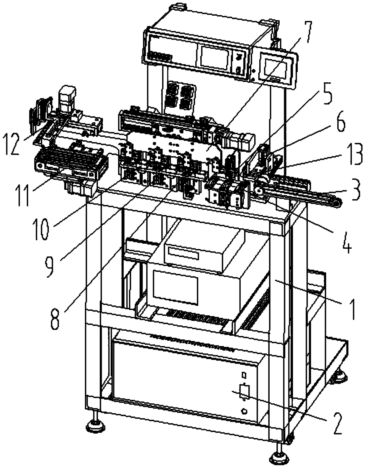
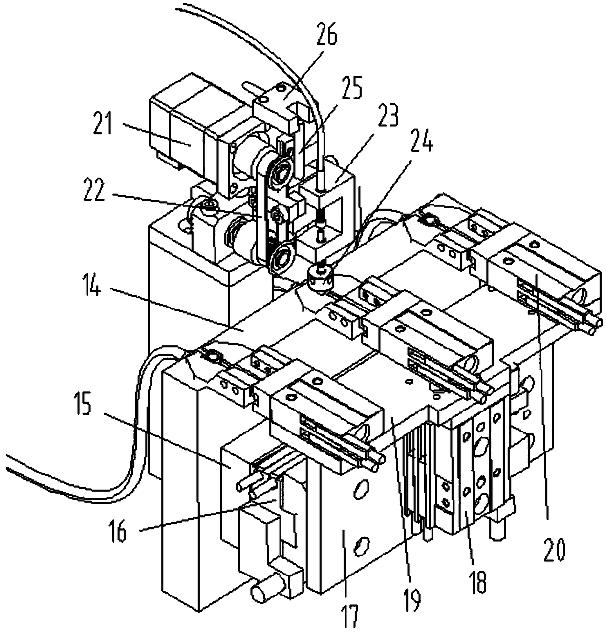
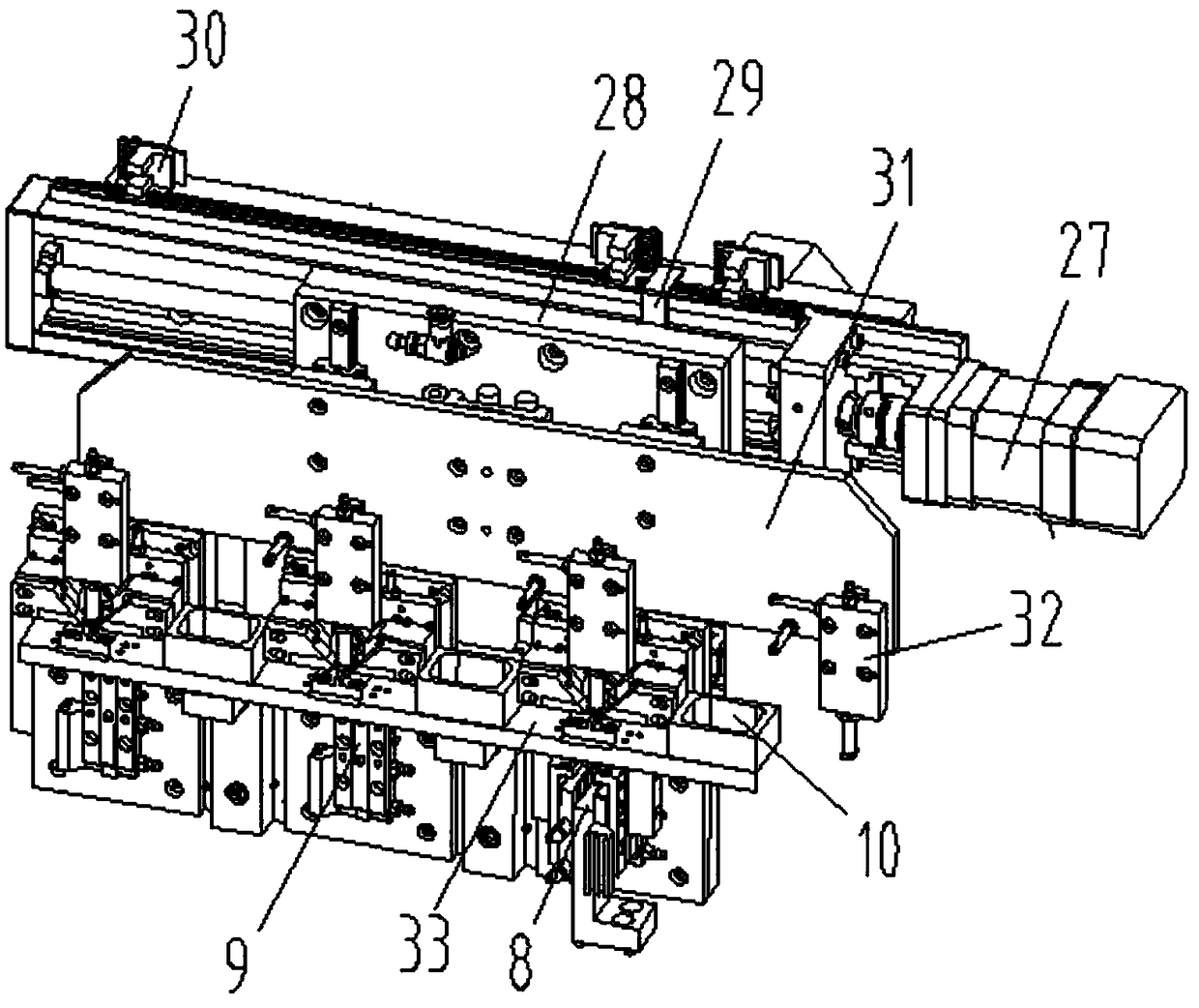
[0032] like Figure 1-Figure 7 As shown, the specific structure of the present invention is: a chip resistance detection and sorting machine, which includes a frame 1 and a power distribution control box 2, and the frame 1 is sequentially provided with feeding and conveying devices from right to left 3. The upper detection seat 14 and the lower detection seat 33, the described feeding conveying device 3 and the upper detection seat 14 cooperate with the upper detection and retrieving device 4, and the upper detection seat 14 and the lower detection seat 33 are taken by the lower detection Cooperate wi...


PUM


Abstract

The invention relates to a chip resistance detection and sorting machine, which includes a frame and a power distribution control box. The frame is provided with a feeding conveying device, an upper detection seat and a lower detection seat in sequence from right to left, and the feeding and conveying device Cooperate with the upper detection seat through the upper detection and reclaiming device, and cooperate with the upper detection seat and the lower detection seat through the lower detection and reclaiming device. The upper detection device that cooperates with the product and uses the CCD detection head as the detection part is arranged above the upper detection seat. The lower detection seat is provided with a lower detection device that cooperates with the lower part of the product. The lower detection device includes a detection discharge seat arranged on the lower detection seat. The lower part of the detection discharge seat is provided with an LCR detection probe that passes through it. The first unqualified product collection box is set on the top, and the invention realizes the automatic and integrated detection of both sides of the chip resistor, which ensures the accuracy of the detection, ensures the quality of the subsequent finished products, and improves the efficiency of detection at the same time.

Description

technical field [0001] The invention relates to the field of detection and sorting of electronic products, in particular to a chip resistance detection and sorting machine. Background technique [0002] After all the processes of chip resistors are completed, they need to be packaged and placed on the carrier tape to form strips. The packaging will bring scraps, mixed materials, vertical materials, reverse materials, stacked materials, empty materials, skipped materials, and material missing corners. , Carrier tape contamination, carrier tape damage, etc.; a bad resistor, flowing to the customer terminal and pasting it on the circuit board, will cause a bad final product, and may even have a potential safety hazard. Therefore, it is necessary to The packaged chip resistors are tested. [0003] In the packaging inspection after the completion of the chip resistor manufacturing process, most of them are for appearance inspection. The traditional method is to inspect the appea...

Claims


Application Information

Patent Timeline
Patent Type & Authority Patents(China)
IPC IPC(8): B07C5/34B07C5/02B07C5/36B07C5/38G01R31/01
CPCB07C5/02B07C5/34B07C5/362B07C5/38B07C2501/0063G01R31/013
Inventor 邓君徐红娇何楚亮
Owner SHENZHEN MESTEK ELECTRONICS CO LTD
Why Eureka
Try Eureka