Shift register, grid drive circuit and driving method thereof, and display device
A technology of shift register and electric potential, which is applied in the field of shift register, gate drive circuit and its drive method, and display device, and can solve problems such as complex circuit structure and input signal interference, and achieve the effect of reducing complexity and avoiding noise
- Summary
- Abstract
- Description
- Claims
- Application Information
AI Technical Summary
Problems solved by technology
Method used
Image
Examples
Embodiment 1
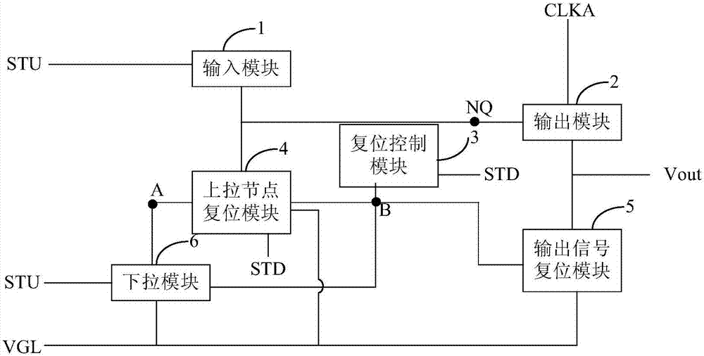
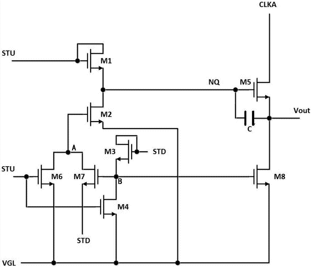
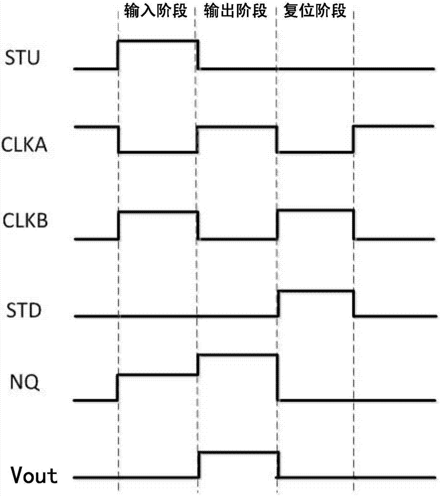
[0063] Please refer to Figure 1 to Figure 3 , this embodiment provides a shift register, including: an input module 1 , an output module 2 , a reset control module 3 , a pull-up node reset module 4 and an output signal reset module 5 .
[0064] The input module 1 is connected to the first signal input terminal STU, the pull-up node reset module 4 and the pull-up node NQ, and is used for precharging the pull-up node NQ under the control of the signal input from the first signal input terminal STU.
[0065] The output module 2 is connected to the first clock signal input terminal CLKA, the pull-up node NQ, the output signal reset module 5 and the signal output terminal Vout, and is used to control the potential of the pull-up node NQ to output the first clock signal input terminal CLKA The input signal is output through the signal output terminal Vout.
[0066] The reset control module 3 is connected to the pull-up node reset module 4, the output signal reset module 5 and the ...
Embodiment 2
[0091] Please refer to Figure 4 and Figure 5 , the present embodiment provides a shift register, which has a structure similar to the shift register of embodiment 1, and its difference from embodiment 1 is that the shift register also includes: a potential maintenance module 7; the potential maintenance module 7 is connected to The second clock signal input terminal CLKB, the first signal input terminal STU, the input module 1, the first clock signal input terminal CLKA and the pull-up node reset module 4 are used to input the first clock signal input terminal CLKA and the second clock signal Under the control of the signal input from the terminal CLKB, the leakage current generated by the pull-up node reset module 4 is prevented.
[0092] It should be noted that CLKA and CLKB are two externally controlled clock signals with opposite logic, that is, when the first clock signal input terminal CLKA outputs a high level, the second clock signal input terminal CLKB outputs a lo...
Embodiment 3
[0112] Please refer to Image 6 , this embodiment provides a gate drive circuit, the gate drive circuit includes a multi-stage shift register in Embodiment 1 or Embodiment 2, and the signal output by the signal output terminal Vout of the shift register in the Nth stage is used as the N+th The input signal of the first signal input terminal STU of the 1st stage shift register; the signal output from the second signal input STD terminal of the Nth stage shift register 10 is connected to the signal output terminal of the N+2th stage shift register.
[0113] It should be noted that the signal output from the signal output terminal Vout of each stage of the shift register is used to drive the gate line G connected to the display area of the display panel.
[0114] The gate driving circuit of this embodiment includes the multi-stage shift register of Embodiment 1 or Embodiment 2. For a detailed description, reference may be made to the shift register of Embodiment 1 or Embodiment...
PUM
 Abstract
Description
Claims
Application Information


