

Array substrate, liquid crystal display panel and display device
A technology of array substrates and thin film transistors, applied in optics, instruments, electrical digital data processing, etc., can solve problems such as crosstalk of display devices and large influence of data lines, and achieve the goal of improving crosstalk, improving disconnection problems, and improving yield Effect
- Summary
- Abstract
- Description
- Claims
- Application Information
AI Technical Summary
Problems solved by technology
Method used
Image

Examples
Embodiment Construction
[0021] The present invention will be further described in detail below in conjunction with the accompanying drawings and embodiments. It should be understood that the specific embodiments described here are only used to explain the present invention, but not to limit the present invention. In addition, it should be noted that, for the convenience of description, only some structures related to the present invention are shown in the drawings but not all structures.
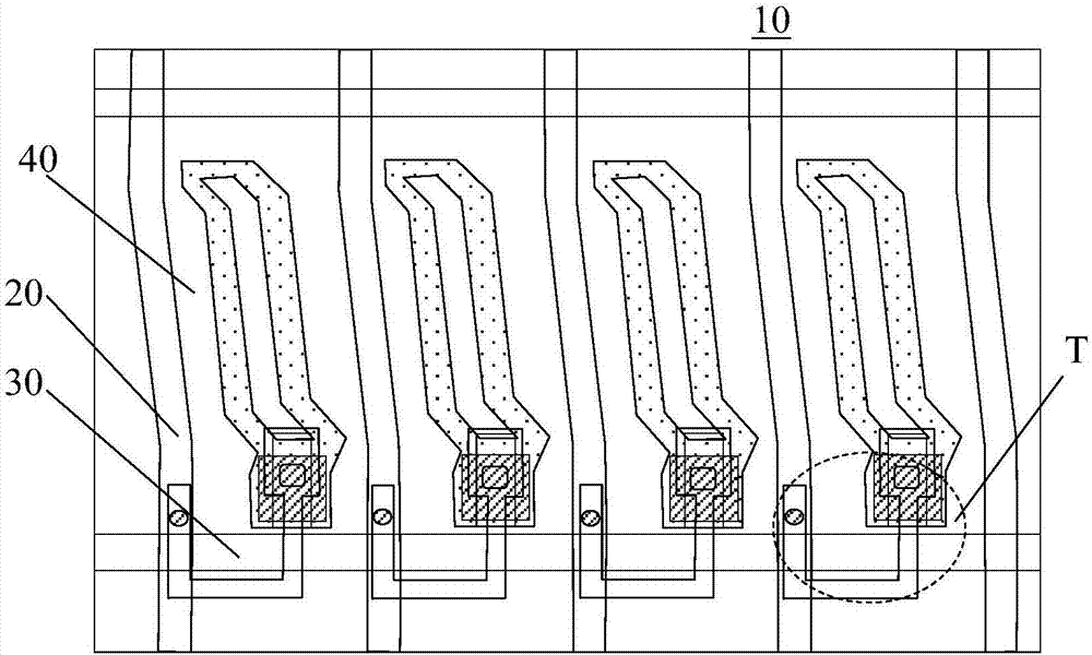
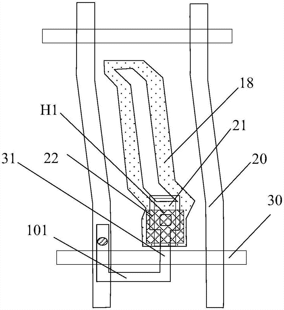
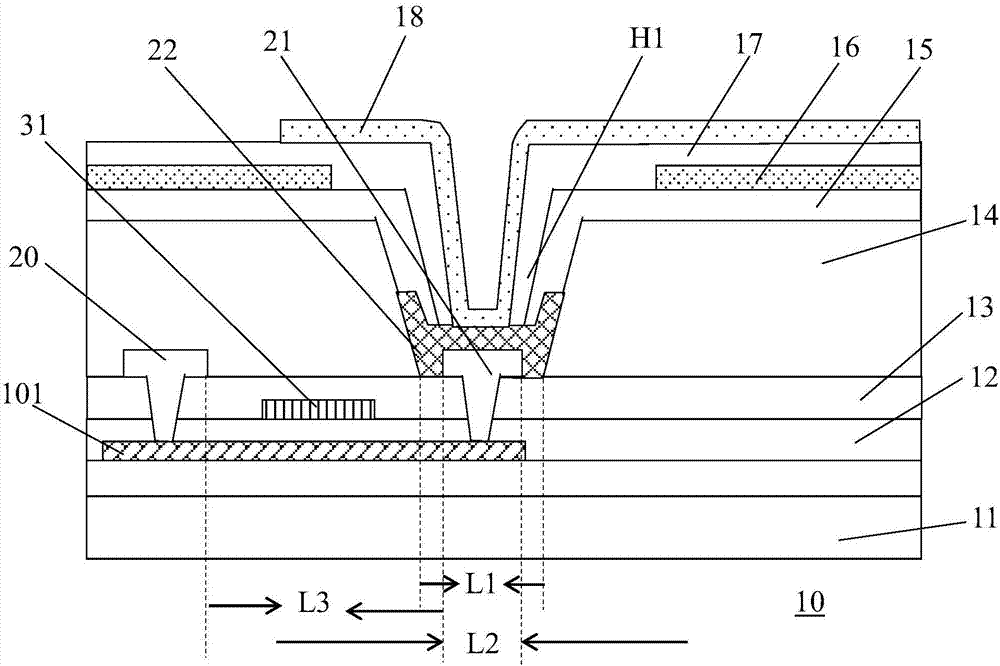
[0022] Embodiments of the present invention firstly provide an array substrate, such as figure 1 and figure 2 as shown, figure 1 is a schematic diagram of an array substrate provided in an embodiment of the present invention, figure 2 yes figure 1 A schematic diagram of a single pixel unit in the array substrate shown. The array substrate 10 includes a plurality of data lines 20 and a plurality of scan lines 30, the plurality of data lines 20 and the plurality of scan lines 30 are intersected to define a plu...
PUM
 Abstract
Description
Claims
Application Information