A liquid crystal display panel and display device

A liquid crystal display panel, flat technology, applied in instruments, nonlinear optics, optics, etc., can solve problems such as poor yellowing of liquid crystal display panels

Active Publication Date: 2020-11-27
SHANGHAI AVIC OPTOELECTRONICS
View PDF13 Cites 0 Cited by
  • Summary
  • Abstract
  • Description
  • Claims
  • Application Information

AI Technical Summary

Problems solved by technology

During the bonding process of liquid crystal display panels, due to imperfect process conditions and various unavoidable human errors, there will be alignment deviations between the color filter substrate and the array substrate. For example, when the preset main support column and the setting When the touch signal lines above the source of the thin film transistors in the array substrate are overlapped and aligned, due to the alignment deviation between the color filter substrate and the array substrate during the lamination process, the main support column and the array substrate may be at a lower level. contact with the plane of the touch signal line, that is, relative to the preset contact and support plane above the touch signal line, after the alignment deviation occurs, the lower plane on the array substrate will be attached to the main support after the lamination is completed. The pillars contact and provide support, which will cause more than the actual number of liquid crystal molecules dripped or injected between the color filter substrate and the array substrate, resulting in yellowish defect (Mura) of the liquid crystal display panel.

Method used


Image

  • A liquid crystal display panel and display device
  • A liquid crystal display panel and display device
  • A liquid crystal display panel and display device

Examples


Embodiment Construction

[0030] In order to make the above objects, features and advantages of the present invention more comprehensible, the present invention will be further described below in conjunction with the accompanying drawings and embodiments.

[0031] It should be noted that in the following description, specific details are set forth in order to fully understand the present invention. However, the present invention can be implemented in many other ways than those described here, and those skilled in the art can make similar extensions without departing from the connotation of the present invention. Accordingly, the present invention is not limited to the specific embodiments disclosed below.

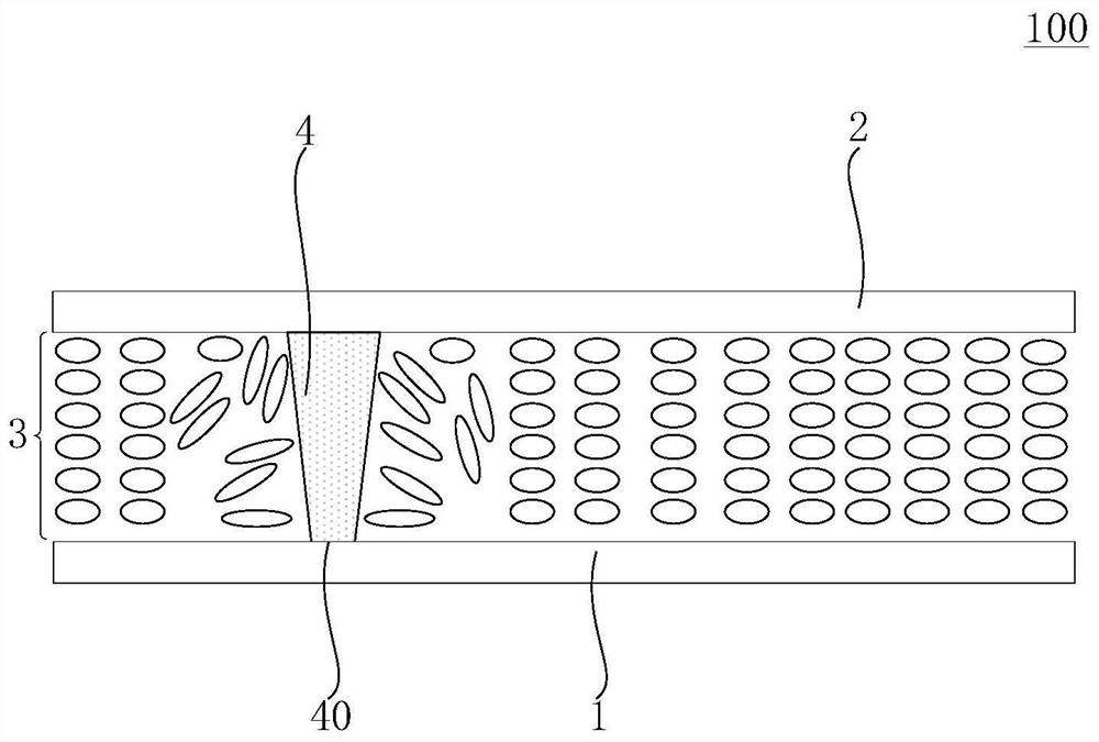
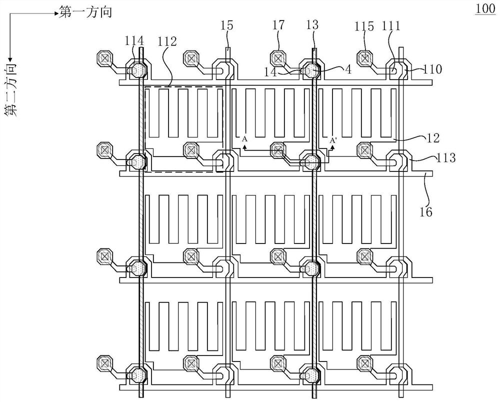
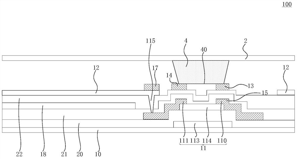
[0032] Figure 1A A schematic structural diagram of a display panel provided by an embodiment of the present invention; Figure 1B A schematic diagram of a partial top view structure of a display panel provided by an embodiment of the present invention; Figure 1C for Figure 1B A schematic cross...


PUM


Abstract

The invention provides a liquid crystal display panel and a display device and relates to the technical field of display. The liquid crystal display panel comprises a color film substrate, an array substrate and a liquid crystal molecular layer. The array substrate comprises an underlayer substrate, multiple thin film transistors and multiple pixel electrodes. The thin film transistors comprise source electrodes and drain electrodes. Multiple touch signal lines overlapped with the source electrodes and multiple first backers overlapped with the drain electrodes are arranged in the direction vertical to the plane where the underlayer substrate is located. The first bottom faces, close to the array substrate, of main supporting columns are overlapped with the positions where the touch signal lines and the source electrodes are overlapped and the positions where the first backers and the drain electrodes are overlapped in the direction vertical to the plane where the underlayer substrate is located. According to the technical scheme, it can be guaranteed that the thickness of a liquid crystal box is unchanged after a contraposition bias is generated, dripping or injection of excessive liquid crystal molecules is avoided, and yellowish badness is avoided.

Description

technical field [0001] The invention relates to the field of display technology, in particular to a liquid crystal display panel and a display device. Background technique [0002] With the continuous development and progress of technology and culture, liquid crystal display technology has replaced CRT picture tube technology to become the mainstream in the field of display, and with the increasing demand for "human-computer interaction", the embedded (In-cell) technology in liquid crystal display technology ) Touch technology has attracted more and more attention. In the prior art, a plurality of main support pillars (MPS, Main Photo Spacer) are generally arranged between the color filter (CF, Color Filter) substrate and the array substrate of the liquid crystal display panel to support the cell of the laminated liquid crystal display panel. In the process of liquid crystal dropping or injection, a fixed number of liquid crystal molecules will be filled between the color f...

Claims


Application Information

Patent Timeline
Patent Type & Authority Patents(China)
IPC IPC(8): G02F1/1339
CPCG02F1/13394
Inventor 朱雪婧金慧俊敦栋梁罗海滨徐伟
Owner SHANGHAI AVIC OPTOELECTRONICS
Why Eureka
Try Eureka