
Thin film transistor array substrate and liquid crystal display device

A thin-film transistor and array substrate technology, which is applied in the field of thin-film transistor array substrates and liquid crystal display devices, can solve problems such as high cost, high power consumption, and difficult implementation, so as to reduce standing angle, save power consumption, and improve light transmission rate effect

Active Publication Date: 2017-08-18
KUSN INFOVISION OPTOELECTRONICS
View PDF4 Cites 0 Cited by
  • Summary
  • Abstract
  • Description
  • Claims
  • Application Information

AI Technical Summary

Problems solved by technology

However, with these technical solutions, there are problems such as difficulty in implementation, high cost, and high power consumption.

Method used


Image

  • Thin film transistor array substrate and liquid crystal display device
  • Thin film transistor array substrate and liquid crystal display device
  • Thin film transistor array substrate and liquid crystal display device

Examples


no. 1 example

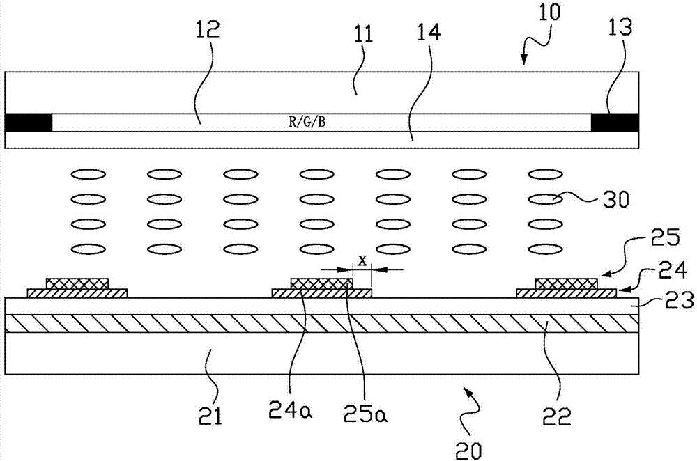
[0027] figure 1 It is a schematic cross-sectional structure diagram of a liquid crystal display device in the first embodiment of the present invention. The liquid crystal display device includes a color filter substrate 10 and a thin film transistor array substrate 20 disposed opposite to each other and a liquid crystal layer 30 sandwiched between them. For clarity, figure 1 2 only shows a schematic diagram of the cross-sectional structure of the liquid crystal display device corresponding to one of the sub-pixels (the R sub-pixel is taken as an example in the figure).

[0028] The structure of the color filter substrate 10 may not be limited. In this embodiment, the color filter substrate 10 includes a first substrate 11, and the first substrate 11 is provided with R, G, B three-color filter film 12 and light-shielding layer (BM) 13, light-shielding layer 13 is arranged between the light-shielding film 12 of different colors, is provided with flat layer (OC) 14 on the light...

no. 2 example

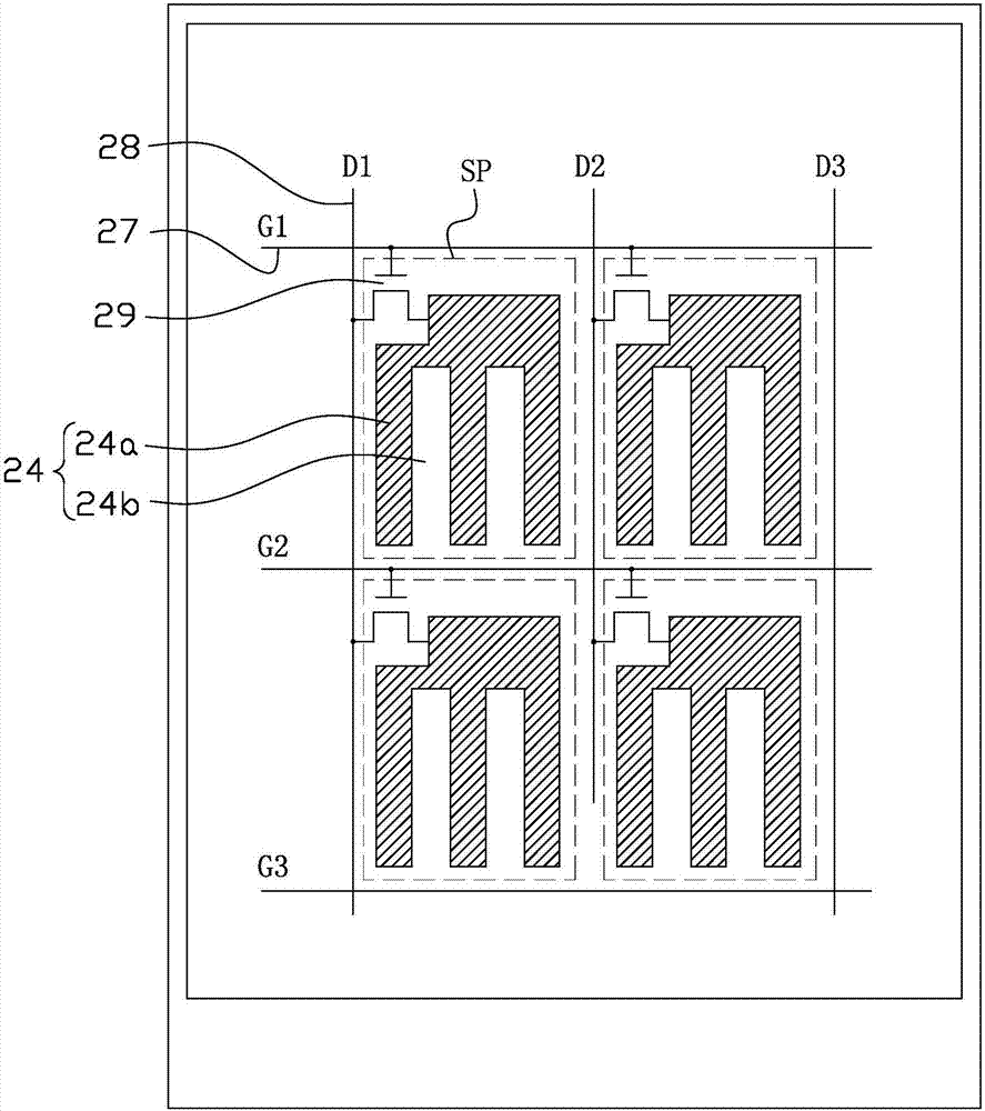
[0046] Figure 5 It is a schematic cross-sectional structure diagram of a liquid crystal display device in the second embodiment of the present invention, Figure 6 for Figure 5 For the schematic diagram of the circuit of the liquid crystal display device, please refer to Figure 5 and Figure 6 The main difference between this embodiment and the above-mentioned first embodiment is that the first electrode 22 in this embodiment is a pixel electrode, and the second electrode 24 is a common electrode, that is, the pixel electrode arranged in each sub-pixel is planar The first electrode 22 of the structure is electrically connected to the drain of the TFT 29 .

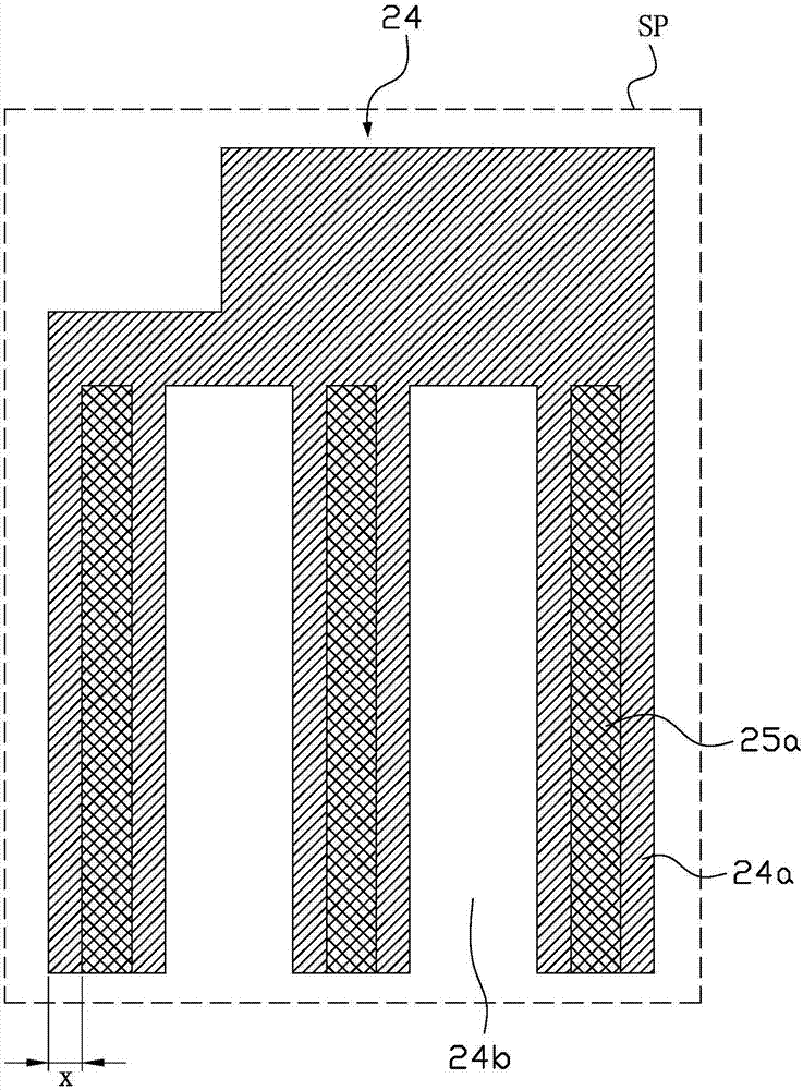
[0047] Figure 7 for Figure 5 The schematic diagram of the plane structure of the second electrode and the insulating protective layer, please combine Figure 7 In this embodiment, the second electrode 24 serving as a common electrode includes a plurality of electrode strips 24a spaced apart from each other in eac...


PUM


Abstract

The invention discloses a thin film transistor array substrate and a liquid crystal display device. The thin film transistor array substrate comprises a first electrode, a first insulation layer and a second electrode, all of which are arranged on a substrate. The second electrode is located above the first electrode. The first insulation layer is clamped between the first electrode and the second electrode. The first electrode is of a planar structure. The second electrode is of a stripped structure and comprises multiple electrode strips which are mutually spaced. The second electrode is provided with a second insulation layer. The second insulation layer comprises multiple insulation strips which are mutually spaced. The multiple insulation strips are arranged on the multiple electrode strips in a one-to-one correspondence mode. Each insulation strip extends along the length direction of a corresponding electrode strip. By making a layer of insulation and protection layer above the second electrode, a vertical electric field above the second electrode is undermined. The standing angle of positive dielectric anisotropy above the second electrode is reduced when an FFS-type liquid crystal display device displays. Therefore, light transmissivity of positive dielectric anisotropy is improved.

Description

technical field [0001] The invention relates to the field of display technology, in particular to a thin film transistor array substrate and a liquid crystal display device. Background technique [0002] Liquid crystal display (liquid crystal display, LCD) has the advantages of good image quality, small size, light weight, low driving voltage, low power consumption, no radiation and relatively low manufacturing cost, and occupies a dominant position in the field of flat panel display. The liquid crystal display device includes a color filter substrate and a thin film transistor array substrate oppositely arranged, and a liquid crystal layer sandwiched between them. [0003] In a traditional Twisted Nematic (TN) liquid crystal display device, the first electrode and the second electrode are respectively formed on two different upper and lower substrates, but the viewing angle of the TN liquid crystal display device is relatively narrow. In order to realize a wide viewing ang...

Claims


Application Information

Patent Timeline
Patent Type & Authority Applications(China)
IPC IPC(8): G02F1/1343G02F1/1368G02F1/1333H01L27/12
CPCG02F1/133345G02F1/134309G02F1/1368G02F1/134372H01L27/1248
Inventor 王新刚
Owner KUSN INFOVISION OPTOELECTRONICS
Learn More