Liquid crystal display device and manufacturing method thereof

A liquid crystal display device and liquid crystal layer technology, applied in nonlinear optics, instruments, optics, etc., can solve problems such as lengthening process time, poor friction process, and reducing dark state brightness, so as to reduce production costs and prevent static moiré (Mura, the effect of enhancing the center contrast

Active Publication Date: 2013-10-16
KUSN INFOVISION OPTOELECTRONICS
View PDF7 Cites 56 Cited by
  • Summary
  • Abstract
  • Description
  • Claims
  • Application Information

AI Technical Summary

Problems solved by technology

[0006] In order to obtain high-contrast, wide-viewing-angle products, and to prevent pollution caused by the contact between the alignment film and the color-resist material of the photoresist layer, resulting in poor rubbing process, the prior art is usually coated after the color-resist material of the color filter substrate is completed. A layer of protective film (overcoat layer, hereinafter referred to as "OC layer") is used as a flat layer, and the alignment film is formed on the OC layer, so that the OC layer will smooth out the discontinuity of the color-resist material in the overlapping area, thereby reducing the gap on the alignment film. The pretilt angle of the liquid crystal molecules achieves the purpose of reducing the brightness of the dark state, increasing the contrast, and increasing the viewing angle. However, due to the need to add an OC layer, the process will increase the process and lengthen the time of the entire process, resulting in production costs. increase

Method used


Image

  • Liquid crystal display device and manufacturing method thereof
  • Liquid crystal display device and manufacturing method thereof
  • Liquid crystal display device and manufacturing method thereof

Examples


Embodiment Construction

[0032] In order to make the above objects, features and advantages of the present invention more comprehensible, specific implementations of the present invention will be described in detail below in conjunction with the accompanying drawings.

[0033] It should be noted that, for the sake of clarity of illustration, the drawings of the present invention only show structural features related to the inventive point of the present invention, while other structural features are omitted.

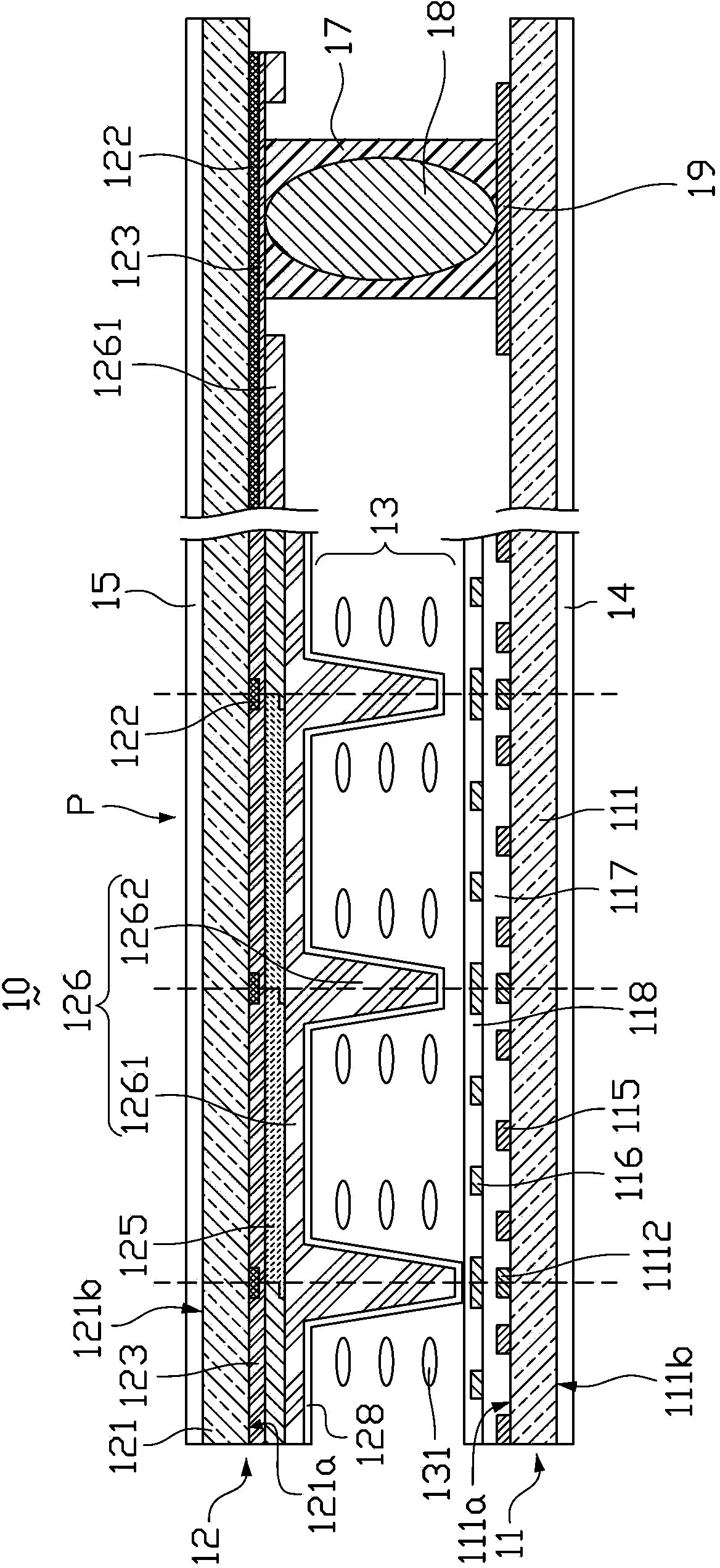
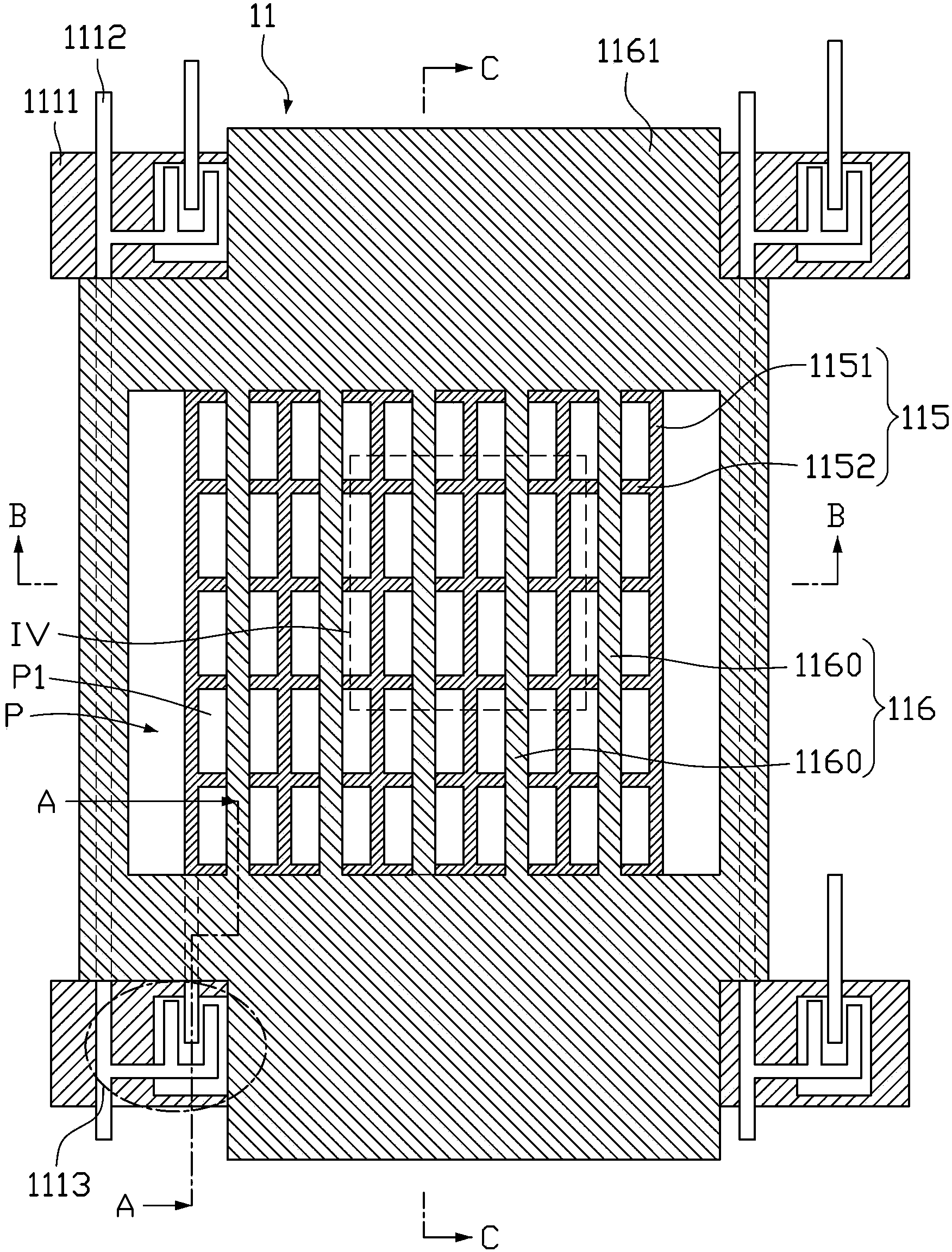
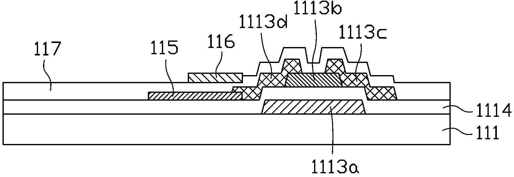
[0034] figure 1 It is a schematic structural diagram of a liquid crystal display device according to an embodiment of the present invention. The liquid crystal display device 10 of the embodiment of the present invention includes an array substrate 11 and a color filter substrate 12 disposed opposite to each other, and a liquid crystal layer 13 sandwiched between the array substrate 11 and the color filter substrate 12 . A plurality of pixel regions P ( figure 1 The area between every two adja...


PUM

PropertyMeasurementUnit
thicknessaaaaaaaaaa

Abstract

The invention discloses a liquid crystal display device. The liquid crystal display device comprises an array substrate, a color film substrate opposite to the array substrate and a liquid crystal layer sandwiched between the array substrate and the color film substrate, wherein the array substrate comprises a first transparent base as well as first electrodes and second electrodes formed on the first transparent base, the first electrodes and the second electrodes are arranged on different layers, and an insulation layer is arranged therebetween; the color film substrate comprises a second transparent base as well as black matrixs formed on the second transparent base, third electrodes, a photoresist layer and optical clearance objects; the third electrodes cover the black matrix and the surface on which the black matrix is not arranged, of the transparent base, the photoresist layer covers the third electrodes, the optical clearance objects cover the photoresist layer, and the optical clearance objects comprise a plane layer covered with the photoresist layer and optical clearances integrally extending from the plane layer and used for providing interval support for the liquid crystal layer; liquid crystal molecules in the liquid crystal layer are negative.

Description

technical field [0001] The invention relates to the technical field of liquid crystal display, in particular to a liquid crystal display device and a manufacturing method thereof. Background technique [0002] Thin Film Transistor-Liquid Crystal Display (TFT-LCD) is widely used in the field of flat panel display because of its low radiation, thin thickness and low power consumption. Initially, most desktop TFT-LCDs adopt TN (Twisted Nematic, twisted nematic) mode. However, the first electrode and the second electrode of the TN type liquid crystal display are respectively formed on the upper and lower substrates, and the liquid crystal molecules It rotates in a plane perpendicular to the substrate. Due to the optical anisotropy of the liquid crystal molecules, the optical path of light entering the human eye after passing through the liquid crystal molecules from different angles is different, so the display effect is different, which will inevitably lead to a relatively smal...

Claims


Application Information

Patent Timeline
Patent Type & Authority Applications(China)
IPC IPC(8): G02F1/1343G02F1/1339G02F1/1335G02F1/1337G02F1/1333
Inventor 钟德镇崔宏青李东朝
Owner KUSN INFOVISION OPTOELECTRONICS
Why Eureka
Try Eureka