Through-hole manufacturing method, display substrate manufacturing method, and display substrate

A manufacturing method and a display substrate technology, which are applied in semiconductor/solid-state device manufacturing, instruments, semiconductor devices, etc., and can solve problems such as the reduction of image display quality of display devices

Active Publication Date: 2017-08-18
BOE TECH GRP CO LTD +1
View PDF10 Cites 5 Cited by
  • Summary
  • Abstract
  • Description
  • Claims
  • Application Information

AI Technical Summary

Problems solved by technology

[0004] The purpose of the present invention is to provide a method for making a via hole, which is used to solve the technical problem that the picture display quality of the display device is reduced due to poor connection between the pixel electrode and the drain electrode

Method used


Image

  • Through-hole manufacturing method, display substrate manufacturing method, and display substrate
  • Through-hole manufacturing method, display substrate manufacturing method, and display substrate
  • Through-hole manufacturing method, display substrate manufacturing method, and display substrate

Examples


Embodiment Construction

[0054] In order to further illustrate the manufacturing method of the via hole, the manufacturing method of the display substrate, and the display substrate provided by the embodiments of the present invention, a detailed description will be given below in conjunction with the accompanying drawings.

[0055] see figure 1 , the manufacturing method of the via hole provided by the embodiment of the present invention includes:

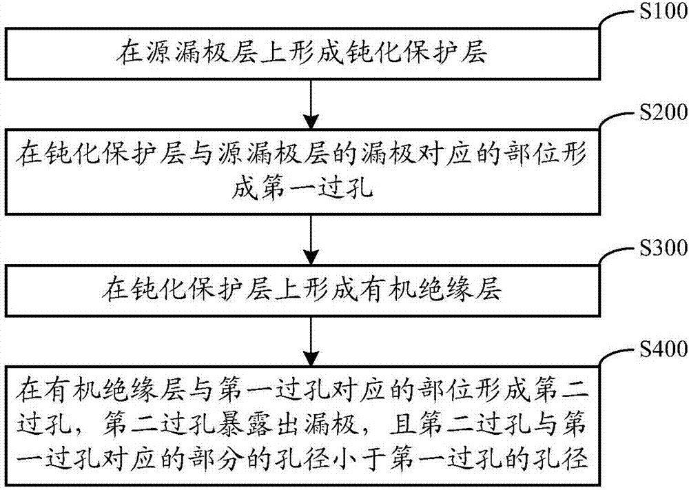
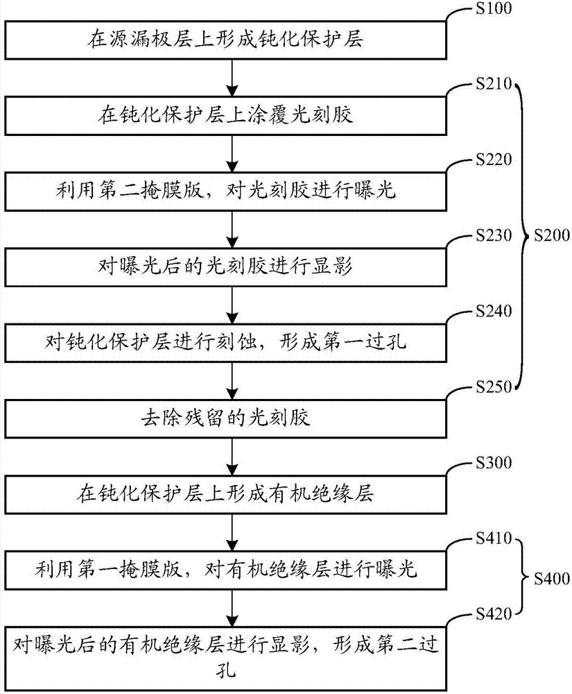
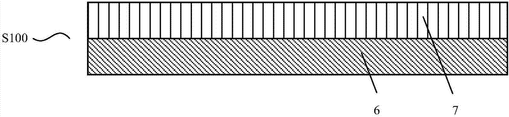
[0056] Step S100 , forming a passivation protection layer on the source and drain layers.

[0057] Step S200 , forming a first via hole at a portion of the passivation protection layer corresponding to the drain of the source and drain layers.

[0058] Step S300, forming an organic insulating layer on the passivation protection layer.

[0059] Step S400, forming a second via hole at the part of the organic insulating layer corresponding to the first via hole, the second via hole exposes the drain electrode, and the diameter of the part of the second via...


PUM


Abstract

The invention discloses a through-hole manufacturing method, a display substrate manufacturing method and a display substrate, which relate to the display manufacturing technology field and aim to solve the problem with the decrease in the quality of the image displaying of a display device caused by the poor connection between the pixel electrode and the drain electrode. The through-hole manufacturing method comprises the following steps: forming a passivation protection layer on a source and drain layer; forming a first through hole on the passivation protection layer at the position corresponding to the source and drain electrode layer of the source and drain layers; forming an organic insulation layer on the passivation protection layer; and forming a second through hole on the organic insulation layer at the position corresponding to the first through hole wherein the drain electrode is exposed by the second through hole and the diameter of the second through hole is smaller than that of the first through hole. With the through hole manufacturing method to form the second through hole, the hole walls of the second through hole all correspond to the organic insulation layer; and the connection between the pixel electrode and the drain electrode through the second through hole is not subjected to disconnection so that the pixel electrode and the drain electrode could be connected well and that the quality of image displaying of a display device is improved.

Description

technical field [0001] The invention relates to the technical field of display manufacturing, in particular to a method for manufacturing a via hole, a method for manufacturing a display substrate, and a display substrate. Background technique [0002] A display device is a device used to display text, numbers, symbols, pictures, or images formed by a combination of at least two of the text, numbers, symbols, and pictures. The display device usually includes a display substrate, and the display substrate usually includes a plurality of pixel units formed on the base substrate and arranged in an array, each pixel unit usually includes a thin film transistor and a pixel electrode located on the side of the thin film transistor away from the base substrate, The pixel electrode is connected to the drain in the source-drain layer of the thin film transistor. [0003] At present, in the display substrate, an insulating layer is usually arranged between the pixel electrode and the...

Claims


Application Information

Patent Timeline
Patent Type & Authority Applications(China)
IPC IPC(8): H01L21/768H01L27/12H01L21/77
CPCH01L27/1244H01L27/1259H01L21/76802G02F1/136227H01L27/124H01L27/1262
Inventor 万云海杨成绍王文龙曹可
Owner BOE TECH GRP CO LTD
Why Eureka
Try Eureka