Wafer growth control apparatus and method

A growth control and wafer technology, applied in semiconductor/solid-state device manufacturing, electrical components, circuits, etc., can solve problems such as warpage and uneven heating of wafers, and achieve the effect of solving warpage

Active Publication Date: 2017-09-15
QINGDAO JASON ELECTRIC
View PDF8 Cites 15 Cited by
  • Summary
  • Abstract
  • Description
  • Claims
  • Application Information

AI Technical Summary

Problems solved by technology

[0005] The present application provides a wafer growth control device and method to solve the technical problem of warpage caused by uneven heating in the epitaxial growth of existing wafers

Method used


Image

  • Wafer growth control apparatus and method
  • Wafer growth control apparatus and method
  • Wafer growth control apparatus and method

Examples


Embodiment Construction

[0023] The specific implementation manners of the present application will be described in further detail below in conjunction with the accompanying drawings.

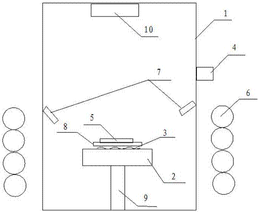
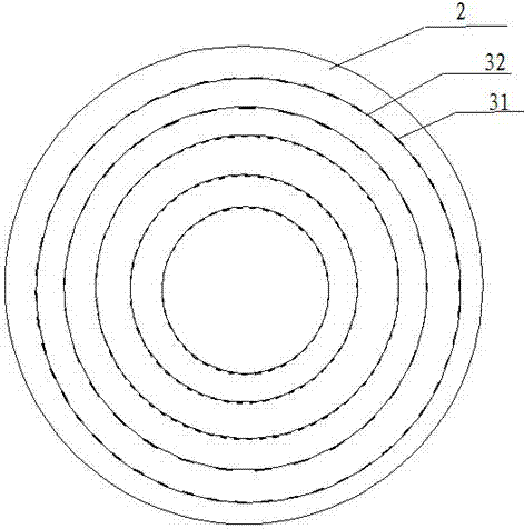
[0024] The wafer growth control device proposed by this application, such as figure 1 As shown, it includes a reaction chamber 1, a base 2 arranged in the reaction chamber, a plurality of annular heating wires 3, a heating controller (not shown in the figure), a warpage measuring instrument 4 and a radio frequency heating coil arranged outside the reaction chamber 6. The wafer 5 is placed on the base 2; a plurality of annular heating wires 3 are concentrically arranged on the upper surface of the base 2, and are all connected to the heating controller.

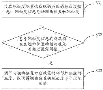
[0025] The RF heating coil 6 is connected to the heating controller, and the heating controller controls the output of strong current to the RF heating coil, so that the RF heating coil generates a magnetic field. During the epitaxial growth process of the wafer, the i...


PUM


Abstract

The invention discloses a wafer growth control apparatus and method. Multiple concentric annular heating wires are arranged on a substrate of a reaction chamber, and a wafer is placed on the substrate; in the epitaxial growth process of the wafer, a heating controller receives warping degree information obtained by a warping degree measurer arranged outside the reaction chamber; and when the controller judges that the wafer suffers from a warping condition exceeding a set threshold value based on the warping degree information, the controller adjusts the temperature of the annular heating wires arranged corresponding to the wafer warping position to be improved or declined, so as to achieve a technical effect of uniform heating of the wafer, adjust the warping degree in the wafer warping position to be less than the set threshold value, and solve the problem of low yield in the epitaxial growth process of the existing wafer caused by uneven heating.

Description

technical field [0001] The invention belongs to the technical field of manufacturing semiconductor integrated circuits, and in particular relates to a wafer growth control device and method. Background technique [0002] Wafer refers to the silicon wafer used in the production of silicon semiconductor integrated circuits. Because of its circular shape, it is called a wafer; it can be processed into various circuit element structures on the silicon wafer, and become an IC with specific electrical functions. product. [0003] Wafer epitaxial growth refers to growing a thin high-resistance epitaxial layer on a low-resistance substrate, which can improve the flexibility of device design and device performance. During the epitaxial growth process, there has always been the problem of warpage and cracks caused by uneven heating of the wafer, resulting in low yield. [0004] The epitaxial growth of the wafer in the prior art is usually carried out by placing the wafer on a base i...

Claims


Application Information

Patent Timeline
Patent Type & Authority Applications(China)
IPC IPC(8): H01L21/67
CPCH01L21/67103H01L21/67288
Inventor 岳金顺张展张国华周德保梁旭东
Owner QINGDAO JASON ELECTRIC
Why Eureka
Try Eureka