Arc gate-drain composite field plate-based current aperture heterojunction device

A compound field and arc technology, applied in the field of microelectronics, can solve the problems that the field plate structure cannot effectively modulate the electric field distribution in the device, the reverse blocking function cannot be realized, and the device performance is not improved in any way, so as to avoid the complex process. The effect of improving the breakdown voltage, increasing the area, and improving the breakdown voltage

Active Publication Date: 2017-09-15
XIDIAN UNIV
View PDF7 Cites 1 Cited by
  • Summary
  • Abstract
  • Description
  • Claims
  • Application Information

AI Technical Summary

Problems solved by technology

However, up to now, there is still no precedent of the field plate structure being successfully applied to GaN-based current aperture heterojunction field effect devices at home and abroad. This is mainly due to the inherent defects in the structure of GaN-based current aperture heterojunction field effect devices. As a result, the strongest electric field peak in the device drift layer is located near the interface between the current blocking layer and the aperture layer, and the electric field peak is far away from the surfaces on both sides of the drift layer, so the field plate structure can hardly play the role of effectively modulating the electric field distribution in the device, even in GaN The field plate structu

Method used


Image

  • Arc gate-drain composite field plate-based current aperture heterojunction device
  • Arc gate-drain composite field plate-based current aperture heterojunction device
  • Arc gate-drain composite field plate-based current aperture heterojunction device

Examples


Embodiment 1

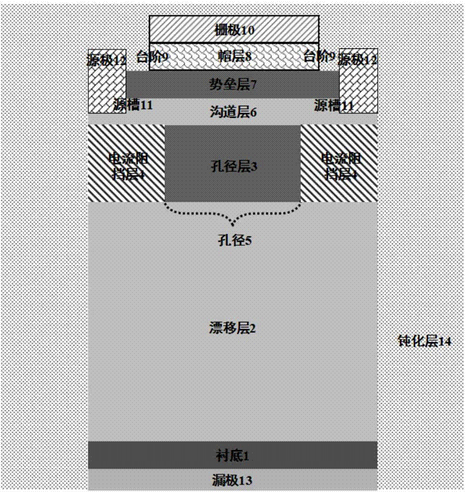
[0073] Embodiment one: using SiO 2 The material is used as a passivation layer to make an arc-shaped gate-drain compound field plate current aperture heterojunction device.

[0074] Step 1. Epitaxial n on substrate 1 - type GaN, forming a drift layer 2, such as image 3 a.

[0075] use n - Type GaN is used as the substrate 1, and the epitaxial thickness is 3 μm and the doping concentration is 1×10 on the substrate 1 by metal organic chemical vapor deposition technology. 15 cm -3 the n - type GaN semiconductor material to form a drift layer 2, wherein:

[0076] The process conditions used for epitaxy are: the temperature is 950°C, the pressure is 40Torr, and the SiH 4 As the doping source, the flow rate of hydrogen gas is 4000 sccm, the flow rate of ammonia gas is 4000 sccm, and the flow rate of gallium source is 100 μmol / min.

[0077] Step 2. Epitaxial n-type GaN on the drift layer to form an aperture layer 3, such as image 3 b.

[0078] Using metal-organic chemical...

Embodiment 2

[0132] Embodiment 2: SiN material is used as a passivation layer to fabricate an arc-shaped gate-drain compound field plate current aperture heterojunction device.

[0133] Step 1. Epitaxial n on substrate 1 - type GaN, forming a drift layer 2, such as image 3 a.

[0134] At a temperature of 1000°C and a pressure of 45Torr, SiH 4 is the dopant source, the flow rate of hydrogen gas is 4400 sccm, the flow rate of ammonia gas is 4400 sccm, and the flow rate of gallium source is 110 μmol / min. - Type GaN is used as the substrate 1, using metal organic chemical vapor deposition technology, the epitaxial thickness is 30 μm on the substrate 1, and the doping concentration is 1×10 17 cm -3 the n - type GaN material to complete the fabrication of the drift layer 2 .

[0135] The second step. Epitaxial n-type GaN on the drift layer to form the aperture layer 3, such as image 3 b.

[0136] At a temperature of 1000°C and a pressure of 45Torr, SiH 4 As the doping source, the flow...

Embodiment 3

[0180] Embodiment 3: Fabricate a curved gate-drain compound field plate current aperture heterojunction device whose passivation layer is SiN.

[0181] Step A. The temperature is 950°C, the pressure is 40Torr, and SiH 4 is the dopant source, the flow rate of hydrogen gas is 4000 sccm, the flow rate of ammonia gas is 4000 sccm, and the flow rate of gallium source is 100 μmol / min. - Type GaN is used as the substrate 1, using metal organic chemical vapor deposition technology, the epitaxial thickness is 50 μm on the substrate, and the doping concentration is 1×1018 cm -3 the n - Type GaN material, making drift layer 2, such as image 3 a.

[0182] Step B. The temperature is 950°C, the pressure is 40Torr, and SiH 4 is the dopant source, the flow rate of hydrogen gas is 4000 sccm, the flow rate of ammonia gas is 4000 sccm, and the flow rate of gallium source is 100 μmol / min. Using metal organic chemical vapor deposition technology, the epitaxial thickness on the drift layer 2 i...


PUM

PropertyMeasurementUnit
Thicknessaaaaaaaaaa
Widthaaaaaaaaaa
Thicknessaaaaaaaaaa

Abstract

The invention discloses an arc gate-drain composite field plate-based current aperture heterojunction device. The heterojunction device comprises a schottky drain (13), a substrate (1), a drifting layer (2), an aperture layer (3), two two-stage-step-structured current blocking layers (4), an aperture (5), a channel layer (6), a barrier layer (7), a cap layer (8) and a gate (10) from the bottom up; stages (9) are etched on the two sides of the cap layer; source grooves (11) are etched in the two sides of the channel layer and the barrier layer; sources (12) are deposited in the source grooves (11); all regions, except the schottky drain bottom, are covered with a passivation layer (14); arc-shaped steps are etched on the upper part and the back surface of the left and right sides of the passivation layer respectively; metal is deposited on the arc-shaped stages to form an arc-shaped gate field plate (15) and an arc-shaped drain field plate (16); and the arc-shaped gate field plate and the arc-shaped drain field plate are electrically connected with the gate and the schottky drain respectively. The heterojunction device has high bidirectional blocking function, low conduction resistance and high rate of finished products, and can be used for a power electronic system.

Description

technical field [0001] The invention belongs to the technical field of microelectronics, and relates to a semiconductor device, in particular to an arc-shaped gate-drain compound field plate current aperture heterojunction device, which can be used in a power electronic system. technical background [0002] Power semiconductor devices are the core components of power electronics technology. As energy and environmental issues become increasingly prominent, research and development of new high-performance, low-loss power devices has become one of the effective ways to improve power utilization, save energy, and alleviate energy crises. In the research of power devices, there is a serious restrictive relationship between high speed, high voltage and low on-resistance. Reasonable and effective improvement of this restrictive relationship is the key to improving the overall performance of the device. With the development of microelectronics technology, the performance of traditio...

Claims


Application Information

Patent Timeline
IPC IPC(8): H01L29/778H01L29/06H01L29/40
CPCH01L29/0615H01L29/0619H01L29/0688H01L29/402H01L29/7786
Inventor 毛维王海永彭紫玲郝跃
Owner XIDIAN UNIV
Why Eureka
Try Eureka