Current aperture heterojunction transistor based on drain field plate and its manufacturing method

A leaky field plate and aperture technology, applied in the field of microelectronics, to achieve the effect of improving yield, simple process and easy realization

Active Publication Date: 2020-04-14
XIDIAN UNIV
View PDF5 Cites 0 Cited by
  • Summary
  • Abstract
  • Description
  • Claims
  • Application Information

AI Technical Summary

Problems solved by technology

However, up to now, there is still no precedent for the successful application of the drain field plate structure in GaN-based current aperture heterojunction transistors at home and abroad.

Method used


Image

  • Current aperture heterojunction transistor based on drain field plate and its manufacturing method
  • Current aperture heterojunction transistor based on drain field plate and its manufacturing method
  • Current aperture heterojunction transistor based on drain field plate and its manufacturing method

Examples


Embodiment 1

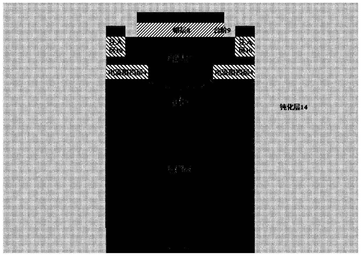
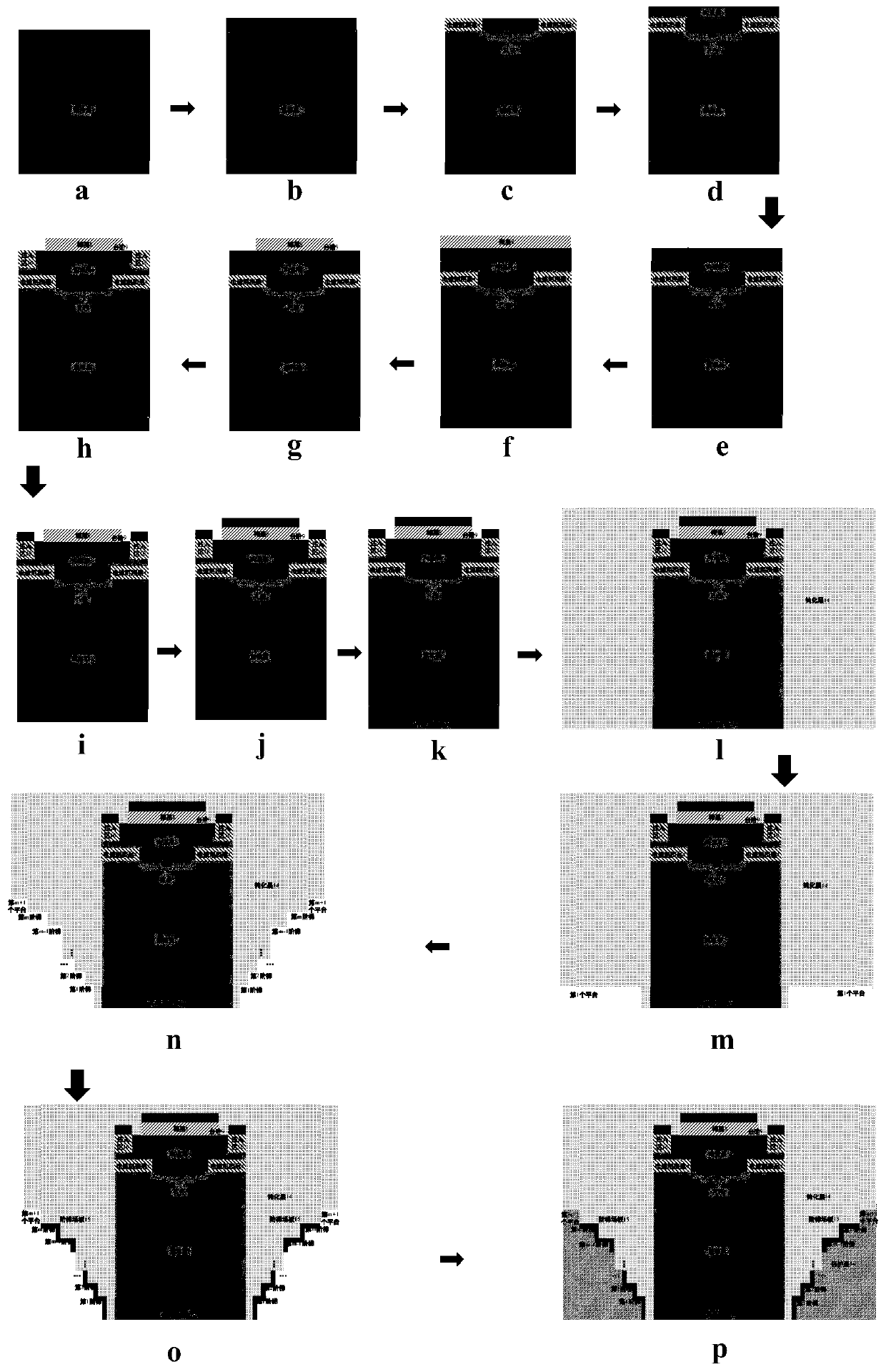
[0062] Embodiment 1: Fabricate a current aperture heterojunction transistor based on a drain field plate in which both the passivation layer and the protective layer are SiN, and the step number of the step field plate is 1.

[0063] Step 1. Epitaxial n on substrate 1 - type GaN, forming a drift layer 2, such as image 3 a.

[0064] use n - Type GaN is used as the substrate 1, and the epitaxial thickness is 3 μm and the doping concentration is 1×10 on the substrate 1 by metal organic chemical vapor deposition technology. 15 cm -3 the n - type GaN material to form a drift layer 2, wherein:

[0065] The process conditions used for epitaxy are: the temperature is 950°C, the pressure is 40Torr, and the SiH 4 As the doping source, the flow rate of hydrogen gas is 4000 sccm, the flow rate of ammonia gas is 4000 sccm, and the flow rate of gallium source is 100 μmol / min.

[0066] Step 2. Epitaxial n-type GaN on the drift layer to form an aperture layer 3, such as image 3 b. ...

Embodiment 2

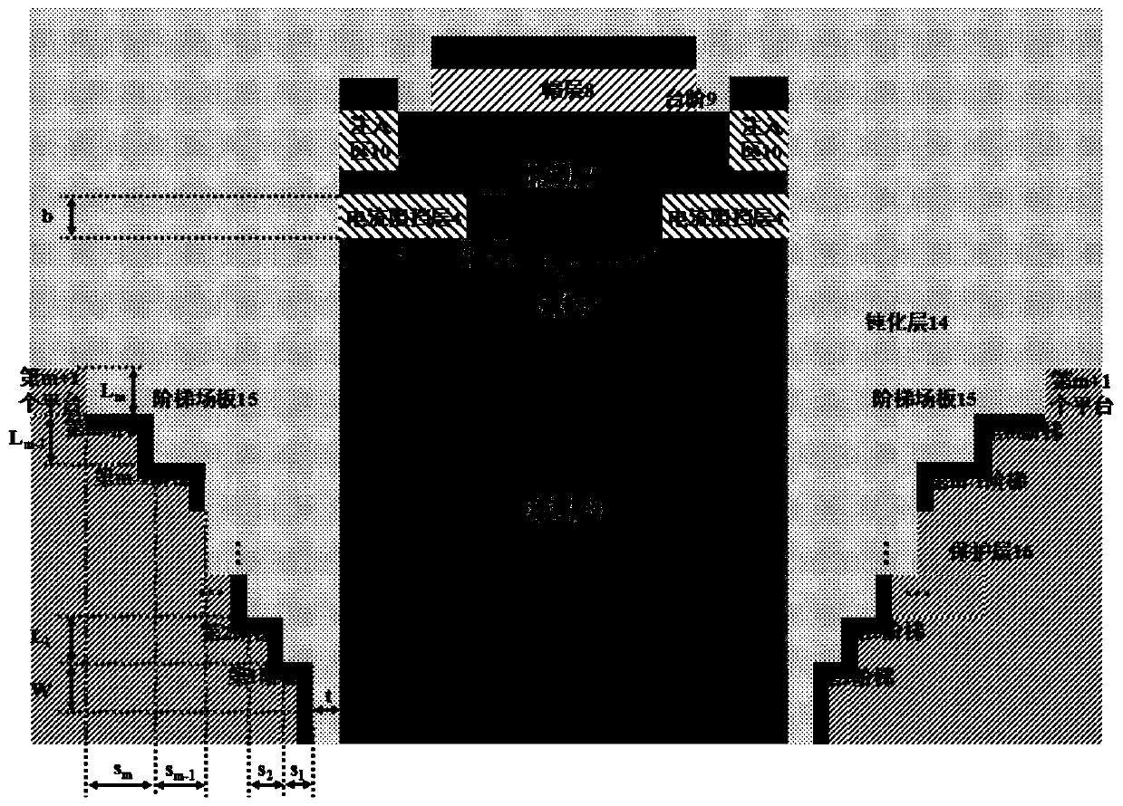
[0116] Embodiment 2: Both the passivation layer and the protective layer are made of SiO 2 , and the number of steps of the stepped field plate is 2, and the current aperture heterojunction transistor based on the drain field plate.

[0117] Step 1. Epitaxial n on substrate 1 - type GaN, forming a drift layer 2, such as image 3 a.

[0118] At a temperature of 1000°C and a pressure of 45Torr, SiH 4 is the dopant source, the flow rate of hydrogen gas is 4400 sccm, the flow rate of ammonia gas is 4400 sccm, and the flow rate of gallium source is 110 μmol / min. - Type GaN is used as the substrate 1, and the epitaxial thickness is 10 μm and the doping concentration is 5×10 15 cm -3 the n - type GaN material to complete the fabrication of the drift layer 2 .

[0119] The second step. Epitaxial n-type GaN on the drift layer to form the aperture layer 3, such as image 3 b.

[0120] At a temperature of 1000°C and a pressure of 45Torr, SiH 4 As the doping source, the flow rat...

Embodiment 3

[0160] Embodiment three: making passivation layer is SiO 2 , the current aperture heterojunction transistor based on the drain field plate, the protective layer is SiN, and the step number of the step field plate is 3.

[0161] Step A. The temperature is 950°C, the pressure is 40Torr, and SiH 4 As the doping source, the flow rate of hydrogen gas is 4000 sccm, the flow rate of ammonia gas is 4000 sccm, and the flow rate of gallium source is 100 μmol / min. - Type GaN is used as the substrate 1, using metal organic chemical vapor deposition technology, the epitaxial thickness is 100 μm on the substrate, and the doping concentration is 1×10 18 cm -3 the n - Type GaN material, making drift layer 2, such as image 3 a.

[0162] Step B. The temperature is 950°C, the pressure is 40Torr, and SiH 4 is the dopant source, the flow rate of hydrogen gas is 4000 sccm, the flow rate of ammonia gas is 4000 sccm, and the flow rate of gallium source is 100 μmol / min. Using metal organic chem...


PUM

PropertyMeasurementUnit
thicknessaaaaaaaaaa
widthaaaaaaaaaa
thicknessaaaaaaaaaa

Abstract

The invention discloses a current aperture hetero-junction transistor based on a drain field plate, and a manufacturing method thereof. The current aperture hetero-junction transistor comprises a substrate (1), a drift layer (2), an aperture layer (3), current blocking layers (4), a channel layer (6) and a barrier layer (7); sources (11) are deposited at two sides of the barrier layer; a cap layer (8) extends on the barrier layer between the sources; steps (9) are carved at two sides of the cap layer; a grid (12) is deposited on the cap layer; an aperture (5) is formed between the two current blocking layers; a Schottky drain (13) is deposited below the substrate; a passivation layer (14) wraps all areas, except the bottom of the Schottky drain; steps are carved at two sides of the back of the passivation layer; metal is deposited on the steps; therefore, a slant field plate (15) is formed; the slant field plate is electrically connected with the Schottky drain; and a protective layer (16) fully fills the bottom of the slant field plate. The current aperture hetero-junction transistor disclosed by the invention has high reverse breakdown voltage, simple process, low conduction resistance and high yield, and can be used for power electronic systems.

Description

technical field [0001] The invention belongs to the technical field of microelectronics and relates to a semiconductor device, in particular to a current aperture heterojunction transistor based on a drain field plate, which can be used in a power electronic system. [0002] technical background [0003] Power semiconductor devices are the core components of power electronics technology. As energy and environmental issues become increasingly prominent, research and development of new high-performance, low-loss power devices has become one of the effective ways to improve power utilization, save energy, and alleviate energy crises. In the research of power devices, there is a serious restrictive relationship between high speed, high voltage and low on-resistance. Reasonable and effective improvement of this restrictive relationship is the key to improving the overall performance of the device. With the development of microelectronics technology, the performance of traditional ...

Claims


Application Information

Patent Timeline
Patent Type & Authority Patents(China)
IPC IPC(8): H01L29/06H01L29/40H01L21/335H01L29/778
CPCH01L29/0615H01L29/404H01L29/66462H01L29/7783H01L29/7786
Inventor 毛维边照科丛冠宇郝跃王冲张进成曹艳荣
Owner XIDIAN UNIV
Why Eureka
Try Eureka