Transistor modeling method based on narrow-pulse small signal measurement

A modeling method, transistor technology, applied in neural learning methods, biological neural network models, special data processing applications, etc., can solve the problem that the small signal equivalent circuit cannot accurately describe the device, the difficulty increases, and the accuracy of the modeling result cannot be guaranteed And other issues

Inactive Publication Date: 2017-09-22
苏州芯智瑞微电子有限公司
View PDF5 Cites 1 Cited by
  • Summary
  • Abstract
  • Description
  • Claims
  • Application Information

AI Technical Summary

Problems solved by technology

However, with the emergence of new materials and new processes, the commonly used small-signal equivalent circuit cannot accurately describe the internal behavior of the device.
For example, gallium nitride transistors with high power density and high heat generation, if the traditional small-signal equivalent circuit is used directly, the non-quasi-static effect, self-heating eff

Method used


Image

  • Transistor modeling method based on narrow-pulse small signal measurement
  • Transistor modeling method based on narrow-pulse small signal measurement
  • Transistor modeling method based on narrow-pulse small signal measurement

Examples


Embodiment Construction

[0030] The present invention will be further described below in conjunction with embodiment.

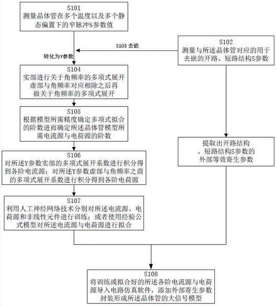
[0031] Such as figure 1 A transistor modeling method based on narrow-pulse small-signal measurements is shown, including the following steps:

[0032] S101 measures the narrow pulse S-parameters of the transistor at multiple temperatures and multiple static biases;

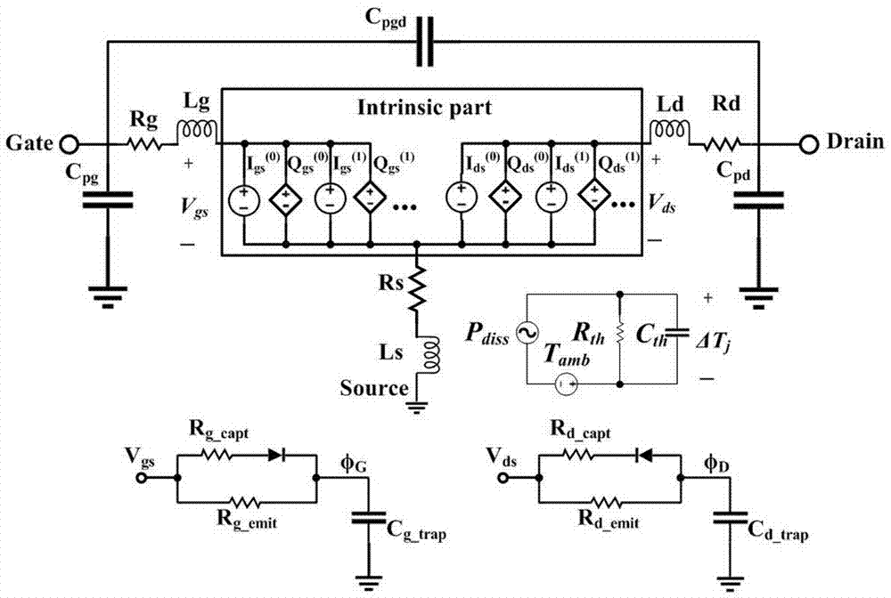
[0033] S102 Measure the S-parameters of the open-circuit structure and the short-circuit structure corresponding to the transistor for de-embedding, and at the same time, extract the external equivalent parasitic parameters of the S-parameters of the open-circuit structure and the short-circuit structure;

[0034] S103 uses the S parameters of the open circuit structure and the short circuit structure to de-embed the narrow pulse S parameters. The specific method is: convert the measured narrow pulse S parameters into Y parameters, and convert the S parameters of the open circuit structure into Y parameters. Convert th...


PUM


Abstract

The invention discloses a transistor modeling method based on narrow-pulse small signal measurement in the field of transistors. The method comprises the following steps of 1, de-embedding: de-embedding an S parameter on the transistor by using an open-circuit\short-circuit structure corresponding to the transistor; 2, extracting an external parameter: extracting an external parasitic parameter from the S parameter of the open-circuit\short-circuit structure; 3, building a constitutive relation: processing the de-embedded S parameter of the transistor, and determining each order of current source and each order of charge source needed by a transistor model; 4, training and fitting: training or fitting the current source and the charge source; and 5, modeling: importing the trained or fit each order of current source and charge source into circuit simulation software, and packaging to form a big signal model of the transistor. According to the method provided by the invention, a small signal equivalent circuit in the transistor is not needed, narrow-pulse small signal measured data is directly used for extracting the constitutive relation between the voltage and current of a port, and thus a complete model of the transistor is built; the method can be used for modeling the transistor.

Description

technical field [0001] The invention relates to a modeling method, in particular to a transistor modeling method. Background technique [0002] High-quality transistor and system models are crucial for computer-aided design (CAD)-based nonlinear microwave-RF circuits, monolithic microwave integrated circuits (MMICs), power amplifiers (PAs), and nonlinear RF systems. With the continuous and rapid development of semiconductor technology and its applications, the power and operating frequency of devices continue to increase, and the transmission of more complex communication signals (such as high standing wave ratio signals of modern communications), the development of high-precision radio frequency devices and system models In order to facilitate the design of semiconductor circuits, it is urgent. [0003] The traditional transistor modeling method is based on the small-signal equivalent circuit of the device, and integrates the parameter values ​​of the equivalent circuit ob...

Claims


Application Information

Patent Timeline
IPC IPC(8): G06F17/50G06N3/08
CPCG06F30/367G06N3/08
Inventor 袁野仲正姚鸿
Owner 苏州芯智瑞微电子有限公司
Why Eureka
Try Eureka