
Voltage-stabilizing semiconductor device for small signals

A semiconductor and small-signal technology, applied in semiconductor devices, semiconductor/solid-state device components, electric solid-state devices, etc., can solve the problems of small amount of solder, poor solder distribution stability, poor precision, etc., to reduce chip costs and avoid product Effects of electrical failure and yield improvement

Inactive Publication Date: 2017-09-26
SUZHOU GOODARK ELECTRONICS CO LTD
View PDF2 Cites 0 Cited by
  • Summary
  • Abstract
  • Description
  • Claims
  • Application Information

AI Technical Summary

Problems solved by technology

[0004] The object of the present invention is to provide a kind of voltage stabilizing semiconductor device for small signal, which adopts specific connecting piece to replace existing 0.4mm size and below chip through the scheme of gold wire and silver glue, from this small signal voltage stabilizing semiconductor device In terms of process design, the technical problems of extremely small amount of solder, poor solder distribution stability and poor precision are solved

Method used


Image

  • Voltage-stabilizing semiconductor device for small signals
  • Voltage-stabilizing semiconductor device for small signals
  • Voltage-stabilizing semiconductor device for small signals

Examples


Embodiment

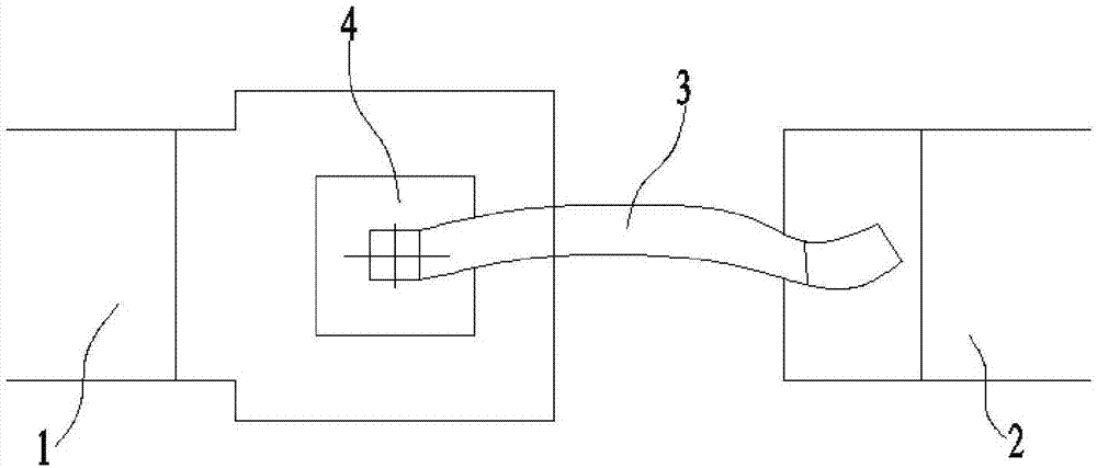
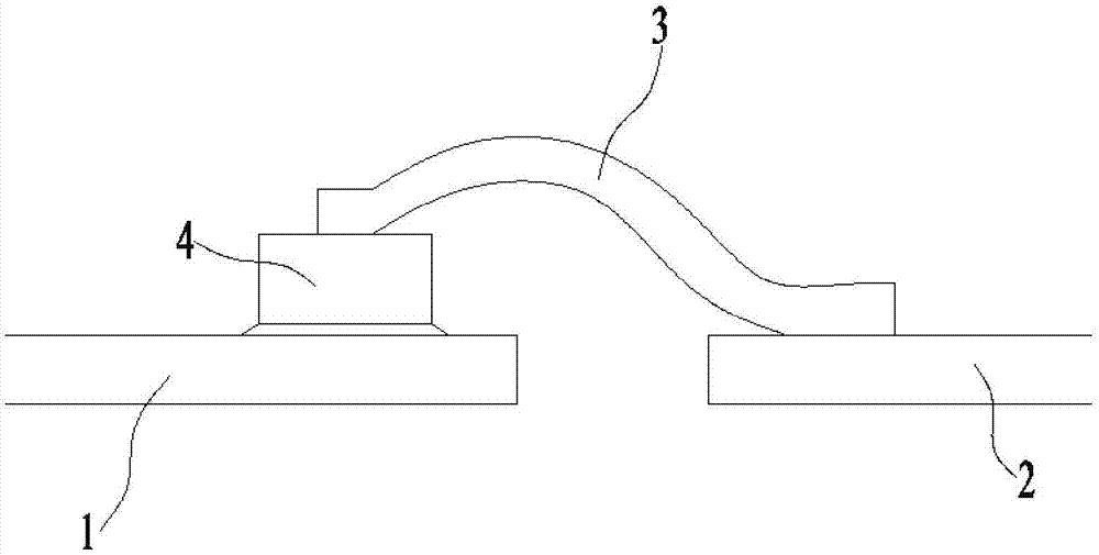
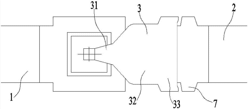
[0020] Embodiment: A voltage stabilizing semiconductor device for small signals, comprising: a first lead bar 1, a second lead bar 2, a connecting sheet 3 and a diode chip 4, and one end of the first lead bar 1 is a support connected to the diode chip 4 Area 12, one end of the diode chip 4 is electrically connected to the supporting area 12 through solder paste, the other end of the first lead bar 1 is the first lead area 11, and the first lead area 11 of the first lead bar 1 is used as the first lead area 11. The current transmission terminal of the rectifier;

[0021] One end of the second lead bar 2 is a welding area 22, the other end of the second lead bar 2 is a second lead area 21, and the second lead area 21 of the second lead bar 2 is used as the current transmission end of the rectifier , the size of the diode chip 4 is 0.3~1mm;

[0022] Between the two ends of the connecting sheet 3 there are successively a strip-shaped area 31, a trapezoidal area 32 and a wide-body...


PUM


Abstract

The invention discloses a voltage-stabilizing semiconductor device for small signals. One end of a first lead wire strip is a support area connected with a diode chip, one end of the diode chip is electrically connected with the support area through soldering paste, the other end of the first lead wire strip is a first pin area, and the first pin area of the first lead wire strip serves as a current transmission end of a rectifier; one end of a second lead wire strip is a welding area, the other area of the second lead wire strip is a second pin area, and the second pin area of the second lead wire strip serves as a current transmission end of the rectifier; a strip-shaped area, a trapezoid area and a broad-body area are formed between two ends of a connecting piece sequentially, and the width of the broad-body area is at least 3 times that of the strip-shaped area; the first welding end located at the tail end of a first bending part is electrically connected with the other end of the diode chip through soldering paste. The specific connecting piece replaces an existing chip in the size of 0.4 mm or below, and the problem of poor solder allocation stability because of very small solder usage is solved from process design by means of gold thread and silver colloid schemes.

Description

technical field [0001] The invention relates to a semiconductor device, in particular to a voltage stabilizing semiconductor device. Background technique [0002] Rectifier / stabilizer devices are widely used in home appliances, office, communication equipment chargers, power supplies and other modules; the chip size of small-signal diode products is extremely small, only about 0.4mm, and it is difficult to realize the mass production of connecting piece technology. The wire bonding structure generally uses gold wire and silver glue, the cost is high, and the wire bonding process is complicated and inefficient. At present, small-signal diode products usually have a wire-bonded structure, which has disadvantages such as low process efficiency and high cost. Due to the extremely small size of the chip and the high difficulty in the process of the connecting sheet structure, it is difficult to achieve mass production. [0003] When designing and developing a semiconductor prod...

Claims


Application Information

Patent Timeline
Patent Type & Authority Applications(China)
IPC IPC(8): H01L23/49
CPCH01L24/36H01L24/40H01L23/49H01L2224/40091H01L2224/40106H01L2224/40177H01L2224/40245H01L2224/48247H01L2224/48091H01L2224/49107H01L2224/73265H01L2924/00014H01L2224/83801H01L2224/84385H01L2224/84801H01L2224/32245H01L24/84H01L24/37H01L2224/73221H01L2224/37099H01L2924/00
Inventor 何洪运程琳
Owner SUZHOU GOODARK ELECTRONICS CO LTD
Learn More