

Array substrate and display panel
An array substrate and display panel technology, applied in nonlinear optics, instruments, optics, etc., can solve the problems of easily damaged substrate related circuits, and achieve the effect of ensuring normal display and reducing the risk of being injured by static electricity.
- Summary
- Abstract
- Description
- Claims
- Application Information
AI Technical Summary
Problems solved by technology
Method used
Image

Examples
Embodiment Construction
[0022] The following will clearly and completely describe the technical solutions in the embodiments of the present invention in conjunction with the accompanying drawings in the embodiments of the present invention. Obviously, the described embodiments are only some of the embodiments of the present invention, not all of them. Based on the embodiments of the present invention, all other embodiments obtained by persons of ordinary skill in the art without making creative efforts belong to the protection scope of the present invention.
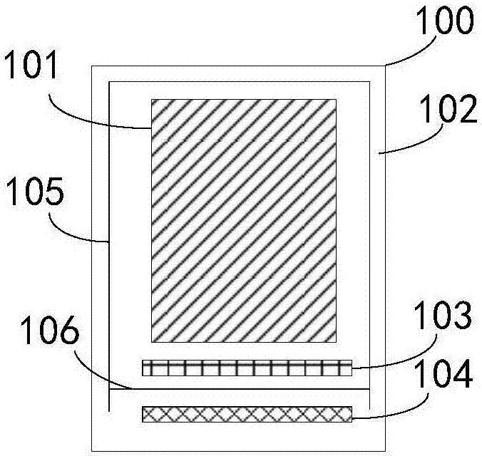
[0023] refer to figure 1 , figure 1 It is a schematic structural diagram of an embodiment of the array substrate of the present invention, and the array substrate 100 includes: a display area 101 and a peripheral area 102 .
[0024] The display area 101 includes thin film transistors ( figure 1 not shown), pixel electrode ( figure 1 Not shown) and other well-known components are not described in detail here.
[0025] Wherein, the peripheral...
PUM
 Abstract
Description
Claims
Application Information