
Fuse and production method thereof

A manufacturing method and fuse technology, which are applied in the manufacture of semiconductor/solid-state devices, electric solid-state devices, semiconductor devices, etc., can solve the problems of increasing production costs, affecting work, and being expensive, so as to save production costs and eliminate possibilities. Effect

Active Publication Date: 2017-10-17
SHANGHAI HUALI MICROELECTRONICS CORP
View PDF3 Cites 5 Cited by
  • Summary
  • Abstract
  • Description
  • Claims
  • Application Information

AI Technical Summary

Problems solved by technology

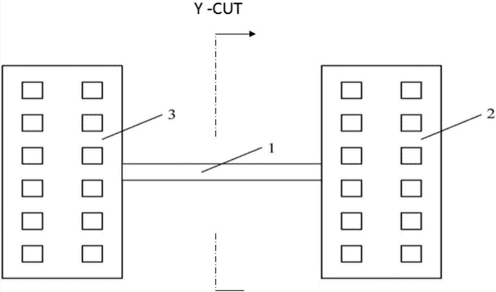
However, there is a problem with the above-mentioned fuse: the moment the fuse is blown, particles will be generated and affect the work of other devices near the Y direction.
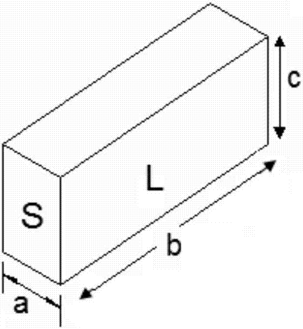
[0008] However, to make the polysilicon fuse width a reach, for example, 60nm and below, a high-end photolithography machine must be used, and the price of this type of photolithography machine is very expensive, which will greatly increase the production cost

Method used


Image

  • Fuse and production method thereof
  • Fuse and production method thereof
  • Fuse and production method thereof

Examples


Embodiment Construction

[0035] The specific embodiment of the present invention will be further described in detail below in conjunction with the accompanying drawings.

[0036] It should be noted that, in the following specific embodiments, in order to clearly show the structure of the present invention for the convenience of explanation, the structures in the drawings are not drawn according to the general scale, and are partially enlarged, deformed and simplified. Therefore, it should be Avoid taking it as a limitation of the present invention to be interpreted.

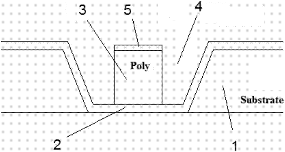
[0037] see image 3 , image 3 It is a schematic cross-sectional structure diagram of a preferred embodiment of the fuse in the polysilicon fuse of the present invention. In the embodiment of the present invention, the same as the prior art, the polysilicon fuse includes a polysilicon fuse and two lead-out ports, and the polysilicon fuse and the two lead-out ports are located on a substrate with an insulating layer.

[0038] The polys...


PUM

PropertyMeasurementUnit
widthaaaaaaaaaa

Abstract

The invention discloses a polycrystalline silicon fuse and the production method thereof. The polycrystalline silicon fuses comprises a polycrystalline silicon fuse link and two leading-out ports. The polycrystalline silicon fuse link comprises a substrate, a first insulation layer, and a polycrystalline silicon melt. The substrate is provided with a groove, and the first insulation layer is disposed on the surface of the substrate provided with the groove in a covered manner. The polycrystalline silicon melt is disposed on the first insulation layer, and is disposed in the groove in an embedded manner. The polycrystalline silicon melt is disposed in the groove in the embedded manner, and then enough safe distances between the melt and other nearby devices are kept, and therefore possible influences of particles formed by fusing of conventional fuses on the nearby devices are effectively eliminated. The key size of the polycrystalline silicon melt is adjusted according to actual requirements, and requirements of a production technology on photolithography and dry etching are low, and therefore the production can be realized by using a common etching machine.

Description

technical field [0001] The invention relates to the technical field of semiconductors, in particular to a structure and a manufacturing method of an embedded polysilicon fuse (fuse). Background technique [0002] A fuse (fuse) refers to an electrical appliance that fuses the fuse with the heat generated by itself and disconnects the circuit when the current exceeds the specified value. The fuse is based on the fact that after the current exceeds the specified value for a period of time, the heat generated by itself melts the melt (fuse), thereby breaking the circuit to make a current protector. Fuse technology is widely used in various programmable logic devices (PLD for short), and generally, fuses can be classified into aluminum fuses and polysilicon fuses (poly fuses). Polysilicon fuse is very suitable for low current because of its easy melting. [0003] Currently, poly fuses in the prior art are usually planar. see figure 1 , figure 1 It shows a schematic structura...

Claims


Application Information

Patent Timeline
Patent Type & Authority Applications(China)
IPC IPC(8): H01L23/525H01L21/768
CPCH01L23/5256H01L21/3065H01L21/32053H01L21/32055H01L21/32135H01L21/32139H01L23/53209H01L23/53271H01L21/76877
Inventor 乔夫龙张强王一许鹏凯
Owner SHANGHAI HUALI MICROELECTRONICS CORP
Learn More