Lead structure of manganese-copper shunt, PCB, and layout structure of PCB
A manganin shunt, PCB board technology, applied in the direction of instruments, measuring devices, measuring electrical variables, etc., can solve the problems of excessive electromagnetic induction current, inaccurate measurement, and meter operation error, so as to increase the loop area, The effect of solving electromagnetic induction mutual interference and preventing sampling interference
- Summary
- Abstract
- Description
- Claims
- Application Information
AI Technical Summary
Problems solved by technology
Method used
Image
Examples
Embodiment 1
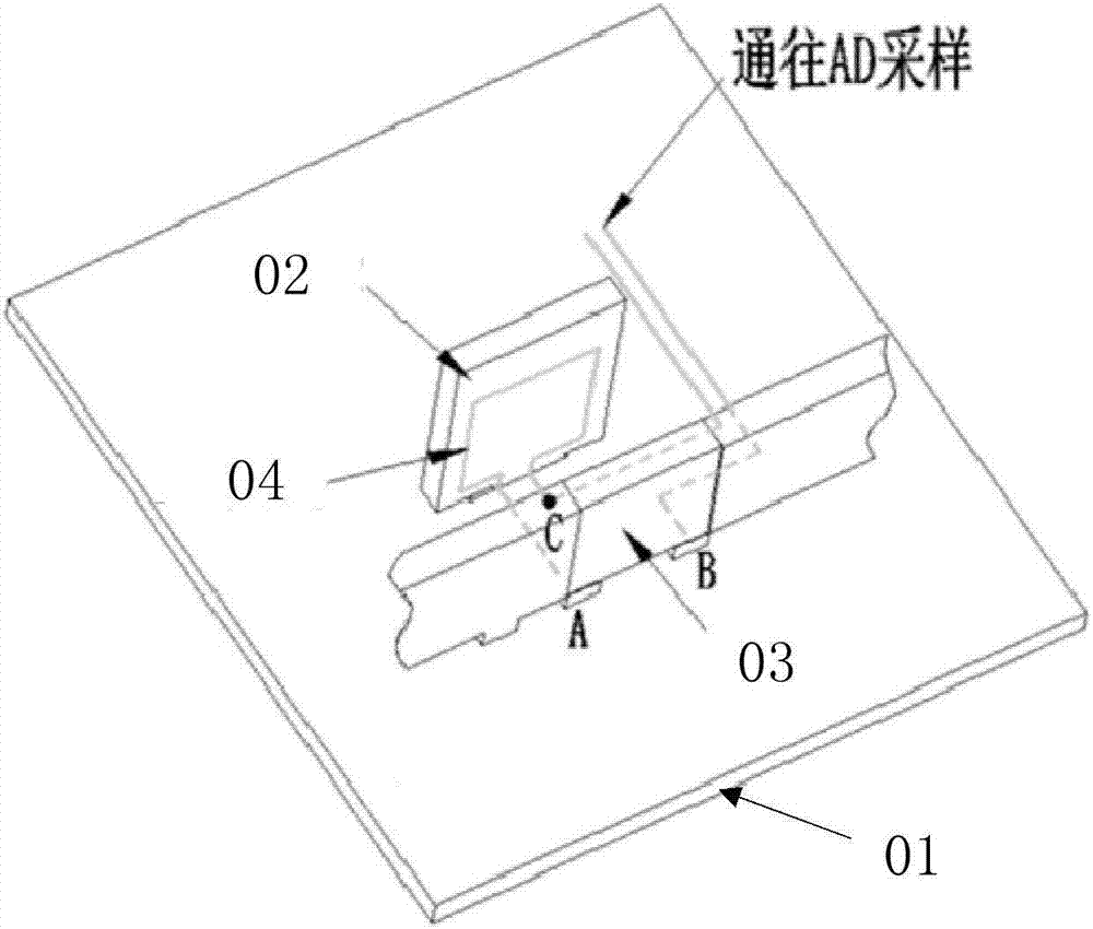
[0039] see figure 1, the design provided in this embodiment adopts the routing structure of the PCB board to resist the interference of the external alternating magnetic field on the manganin shunt, which mainly includes the manganin shunt 03, the first PCB board 01 and the second PCB board 02. The manganin shunt 03 is welded vertically on the first PCB board 01, the second PCB board 02 is parallel to the manganin shunt 03, and the PCB trace goes from the first current sampling point A of the manganin shunt 03 to the second PCB Draw a circular trace 04 on the board 02, and then walk back to point C on the first PCB board 01, and at the same time connect with the PCB trace drawn from the second sampling terminal B of the manganin shunt 03 in parallel or twisted pair To the AD sampling of the chip.
[0040] When there is no second PCB board 02, the alternating magnetic field only acts on the manganin shunt 03, and the induced electromotive force is accumulated on point B, and A...
Embodiment 2
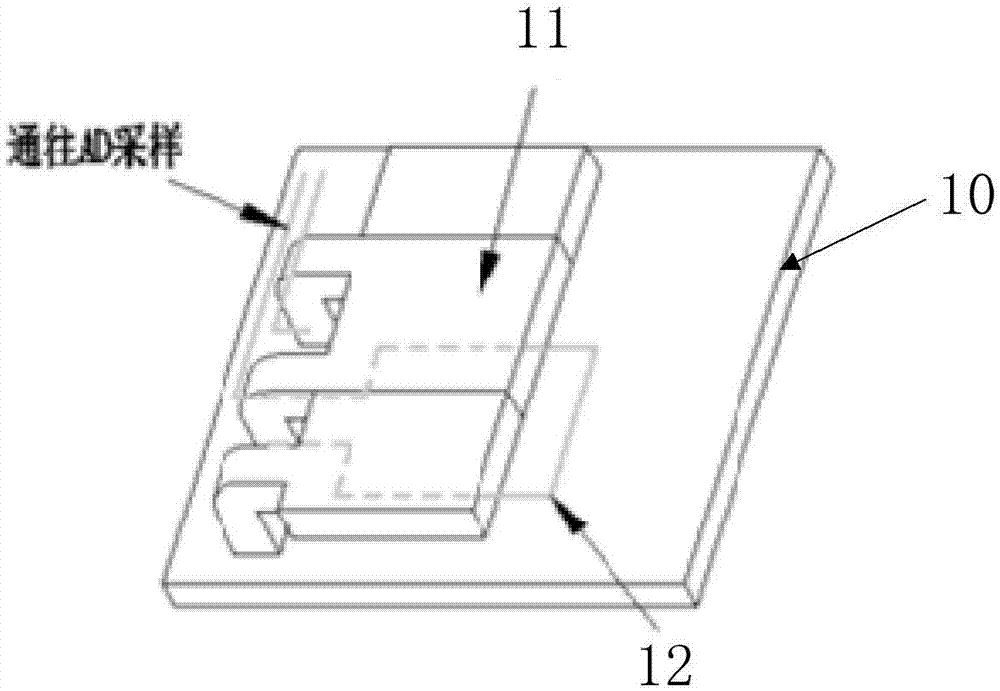
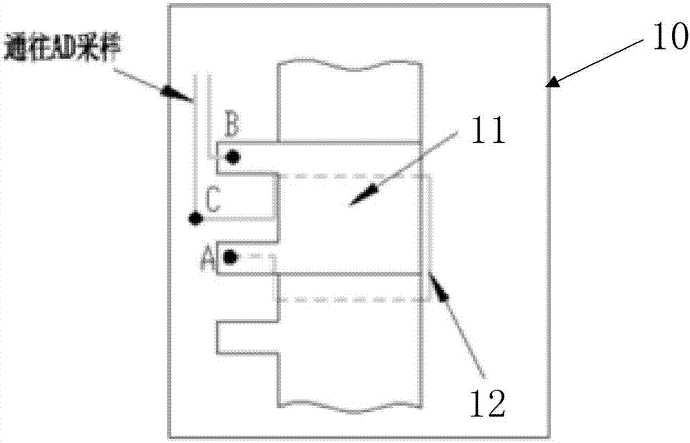
[0043] see figure 2 and image 3 , the design provided in this embodiment adopts the wiring structure of the PCB board to resist the interference of the external alternating magnetic field on the manganin shunt, which mainly includes a sub-PCB board 10 and a manganin shunt 11 . The manganese copper shunt 11 is welded on the PCB board 10 parallel to the PCB board 10, and the PCB trace goes from the first current sampling point A of the manganese copper shunt 11 to the PCB board 10 to draw a circular trace 12, and then walks Go back to point C on the PCB board 10, and at the same time, connect the PCB trace with the second sampling terminal B of the manganin shunt 11 to the AD sampling of the chip in parallel or twisted pair.
[0044] In the same way, this lead structure also accumulates the electromotive force generated by the induced manganin loop at the second current sampling end of the original manganin shunt to the first current sampling end, and the two are accumulated ...
PUM
 Abstract
Description
Claims
Application Information
 - R&D Engineer
- R&D Manager
- IP Professional
- Industry Leading Data Capabilities
- Powerful AI technology
- Patent DNA Extraction
Browse by: Latest US Patents, China's latest patents, Technical Efficacy Thesaurus, Application Domain, Technology Topic, Popular Technical Reports.
© 2024 PatSnap. All rights reserved.Legal|Privacy policy|Modern Slavery Act Transparency Statement|Sitemap|About US| Contact US: help@patsnap.com


