Magnetic film deposition chamber and film deposition device

A magnetic thin film and deposition cavity technology, applied in the field of microelectronics, can solve the problems of not having induced magnetic thin film anisotropy, unable to use magnetic thin film production equipment, etc., to achieve the effect of in-plane anisotropy

Active Publication Date: 2017-11-03
BEIJING NAURA MICROELECTRONICS EQUIP CO LTD
View PDF4 Cites 7 Cited by
  • Summary
  • Abstract
  • Description
  • Claims
  • Application Information

AI Technical Summary

Problems solved by technology

[0004] However, the existing magnetic field-induced deposition methods cannot be applied to production equipment for preparing magnetic thin films, such as PVD equipment
That is to say, the existing film deposition chamber does not have the function of inducing the in-plane anisotropy of the magnetic film

Method used


Image

  • Magnetic film deposition chamber and film deposition device
  • Magnetic film deposition chamber and film deposition device
  • Magnetic film deposition chamber and film deposition device

Examples


Embodiment Construction

[0045] In order to enable those skilled in the art to better understand the technical solution of the present invention, the magnetic film deposition chamber and film deposition equipment provided by the present invention will be described in detail below in conjunction with the accompanying drawings.

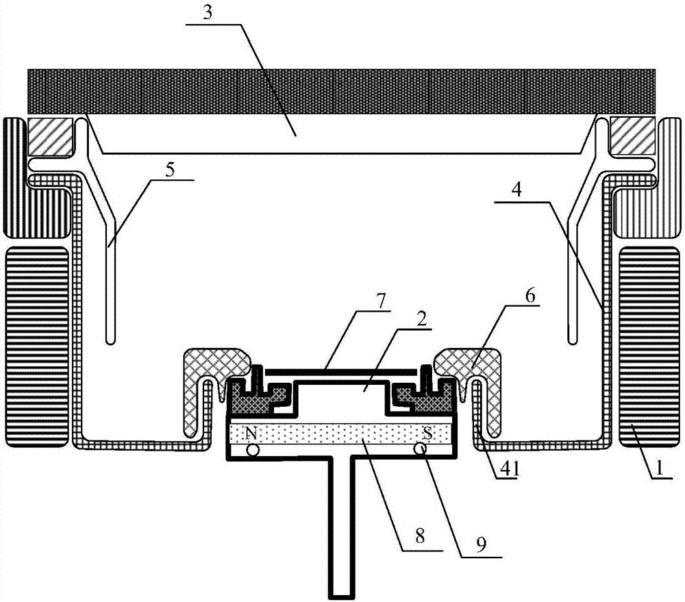
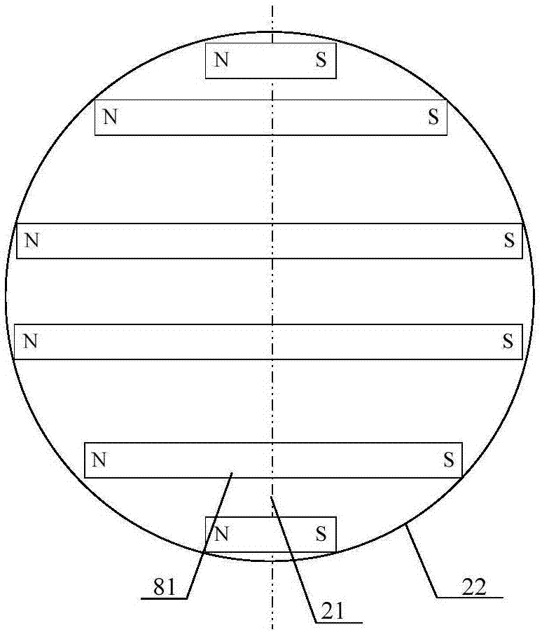
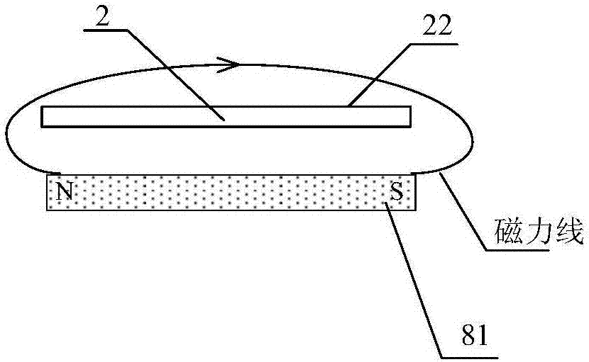
[0046] Please also refer to Figure 1A ~ Figure 1C , the magnetic thin film deposition chamber includes a chamber main body 1 and a shielding assembly, wherein a target 3 is arranged on the top of the chamber main body 1, and in the chamber main body 1 and below the target material 3, a The base 2, the base 2 includes a bearing surface 22 for carrying the workpiece 7 to be processed, the bearing surface 22 is defined to place the workpiece 7 to be processed at a designated position on the base 2, and its shape and size are the same as those of the base 2 The workpiece 7 to be processed has the same shape and size. The above-mentioned shielding assembly includes an upper shieldin...


PUM


Abstract

The invention provides a magnetic film deposition chamber and a film deposition device. The magnetic film deposition chamber comprises a cavity body. The cavity body is internally provided with a base. The base comprises a bearing surface used for bearing a workpiece to be machined. The magnetic film deposition chamber further comprises a bias magnetic field device. The bias magnetic field device comprises a first magnet set. The first magnet set is arranged below the base and used for forming a first horizontal magnetic field above the base. The first horizontal magnetic field is used for enabling a magnetic film deposited on the workpiece to be machined to have in-plane anisotropy. By adopting the magnetic film deposition chamber provided by the invention, the horizontal magnetic field which is enough to induce the in-plane anisotropy can be formed on the base. The requirements for preparing magnetic films with the in-plane anisotropy on large-size workpieces to be machined by production equipment are met.

Description

technical field [0001] The present invention relates to the technical field of microelectronics, in particular to a magnetic thin film deposition chamber and thin film deposition equipment. Background technique [0002] With the development of technology, the integrated circuit manufacturing process can significantly reduce the size of the processor, but there are still some core components such as integrated inductors and noise suppressors that face many difficulties in high frequency, miniaturization, and integration. . In order to solve this problem, soft magnetic thin film materials with high magnetization, high magnetic permeability, high resonance frequency and high resistivity have attracted more and more attention. [0003] Although soft magnetic thin film materials mainly consider its high magnetic permeability and high magnetization strength, as well as low coercive force and low loss, a major factor affecting the development of soft magnetic thin film materials i...

Claims


Application Information

Patent Timeline
IPC IPC(8): C23C14/35H01F41/18
CPCC23C14/351H01F41/18
Inventor 杨玉杰张同文马新艳郑金果王宽冒郭浩贾强
Owner BEIJING NAURA MICROELECTRONICS EQUIP CO LTD
Why Eureka
Try Eureka