A method and system for predicting junction temperature of power devices

A technology for predicting power and devices under test, which is applied in the field of semiconductors, can solve problems such as difficult application, unfavorable practical application and promotion, and complex models, and achieve the effects of accurate prediction of junction temperature, easy implementation and promotion, and strong adaptability

Active Publication Date: 2020-06-19
北京华电锐拓科技有限公司
View PDF7 Cites 0 Cited by
  • Summary
  • Abstract
  • Description
  • Claims
  • Application Information

AI Technical Summary

Problems solved by technology

This type of chip model appears in the semiconductor simulation software TCAD. Based on the process simulation simulation chip manufacturing process, it can fully consider the complex structure of the internal cells of the chip. However, there are tens of thousands of cells inside a chip, and the cells are connected in parallel. The structural model of a cell structure cannot be directly equivalent to the structural model of the chip layer, and it is difficult to combine with external simulation, and the application is difficult
The third is the physical layered model of the chip. This type of chip model is mainly used in the finite element model of the chip. The chip is divided into a depletion layer and an equivalent layer according to the physical structure of the active area and the terminal area. The chip model can study the distribution of electrothermal characteristics inside the chip to a certain extent, but the disadvantage of layering according to the physical structure is that the physical size and boundary conditions of each layer are set based on experience, and there is no corresponding theory as a basis for support. The prediction error is large, and the model is relatively complicated, which is not conducive to practical application and promotion
[0006] In summary, the existing methods based on experimental measurement and the method of simulating and predicting the junction temperature by establishing an equivalent thermal model cannot fully characterize the PN junction temperature inside the chip layer, and the junction temperature prediction error is relatively large.

Method used


Image

  • A method and system for predicting junction temperature of power devices
  • A method and system for predicting junction temperature of power devices
  • A method and system for predicting junction temperature of power devices

Examples


Embodiment 1

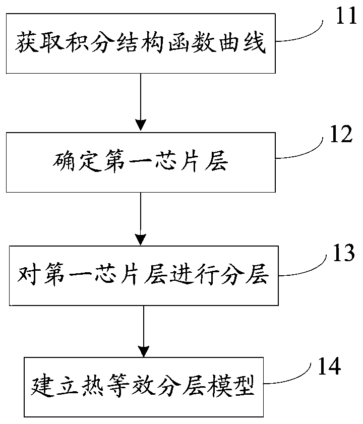
[0061] Such as image 3 As shown, a method to predict the junction temperature of a power device includes:

[0062] Step 11: Obtain the integral structure function curve of the device under test;

[0063] Step 12: Determine the first chip layer of the device under test according to the packaging form of the device under test, the packaging material, and the starting point of the integral structure function curve;

[0064] Step 13: layering the first chip layer according to the slope of the curve segment corresponding to the first chip layer in the integral structure function curve, to obtain each thermal equivalent layer and the corresponding thermal resistance value;

[0065] Step 14: Establishing a thermal equivalent layering model of the chip layer of the device under test according to each thermal equivalent layer and the corresponding thermal resistance value, so as to predict the junction temperature of the device under test.

[0066] Preferably, before performing step...

Embodiment 2

[0078] Such as Figure 4 As shown, a system for predicting the junction temperature of a power device includes:

[0079] Integral curve acquisition module 21, used to acquire the integral structure function curve of the device under test;

[0080] The first chip layer determination module 22 is connected to the integral curve acquisition module, and is used to determine the first chip of the device under test according to the packaging form of the device under test, the packaging material, and the starting point of the integral structure function curve layer;

[0081] The stratification module 23 is connected to the integral curve acquisition module and the first chip layer determination module respectively, and is used to calculate the first chip layer according to the slope of the curve segment corresponding to the first chip layer in the integral structure function curve. A chip layer is layered to obtain each thermal equivalent layer and the corresponding thermal resista...

Embodiment 3

[0095] The application condition of the DC circuit breaker is that the crimping type IGBT device needs to turn off a large current within 3ms, and the heat generated in such a short time is difficult to dissipate through the external radiator, and the heat is mainly concentrated inside the chip, so the chip The modeling of the internal equivalent thermal network is very important for the prediction of junction temperature. In view of the limitations of current chip junction temperature prediction and simulation models in power semiconductor devices, combined with the transient junction temperature prediction requirements of DC circuit breaker application conditions, a method for predicting the junction temperature of power devices provided in this embodiment includes:

[0096] Step 31: Obtain the integral structure function curve and the differential structure function curve of the device under test;

[0097] Step 311: Measure the electrical parameters of the device under test...


PUM


Abstract

The invention discloses a method and a system for predicting a junction temperature of a power device. The method comprises the steps of obtaining an integral structure function curve of a tested device; determining a first chip layer according to a packaging form, a packaging material and a starting point of the integral structure function curve of the tested device; performing layering on the first chip layer according to a slope of a curve segment corresponding to the first chip layer in the integral structure function curve to obtain thermal equivalent layers and corresponding thermal resistance values; and building a thermal equivalent layering model of the chip layer of the tested device according to the thermal equivalent layers and the corresponding thermal resistance values, thereby predicting the junction temperature of the tested device. The thermal equivalent layering model is built for the chip layer by adopting a thermal equivalent layering structure instead of physical layering, so that the thermal equivalent layering model can accurately represent a thermal distribution characteristic of the chip layer in the power semiconductor device; the model can accurately predict the junction temperature of the power device; and the method for building the thermal equivalent layering model is used for all power semiconductor chips, and is convenient to implement and popularize.

Description

technical field [0001] The invention relates to the field of semiconductors, in particular to a method and system for predicting junction temperature of power devices. Background technique [0002] Power semiconductor devices are more and more widely used in power systems, and at least 60% of the world's electric energy is controlled by them. In the future, under the trend of global energy Internet, with large-scale new energy generation and electric vehicles The proportion of mobile unpredictable loads connected to the grid will increase significantly. Therefore, research work on power semiconductor devices has also become a hot spot in recent years, especially high-voltage and high-power semiconductor devices. [0003] Press-connected power semiconductor devices, such as press-connected insulated gate bipolar transistors (Insulated Gate Bipolar Transistor, IGBT), have the advantages of high power density, double-sided heat dissipation, easy series connection and high reli...

Claims


Application Information

Patent Timeline
Patent Type & Authority Patents(China)
IPC IPC(8): G06F30/20
CPCG06F30/20
Inventor 邓二平赵志斌陈杰黄永章
Owner 北京华电锐拓科技有限公司
Why Eureka
Try Eureka