

Substrate and display device
A technology for display devices and substrates, which is applied to electrical components, electrical solid devices, circuits, etc., and can solve problems such as the reduction of light output rate of OLED displays
- Summary
- Abstract
- Description
- Claims
- Application Information
AI Technical Summary
Problems solved by technology
Method used
Image

Examples
Embodiment 1
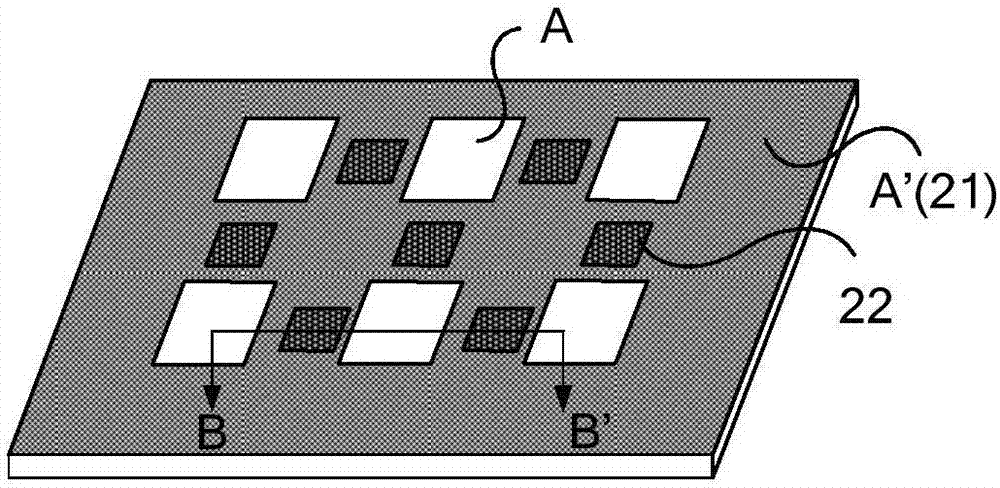
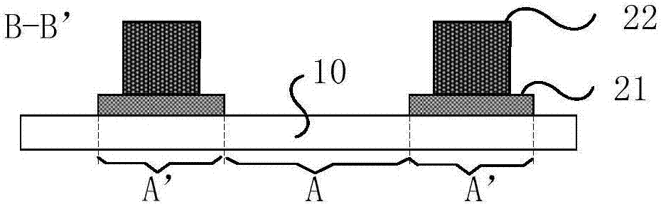
[0032] An embodiment of the present invention provides a substrate, such as figure 2 and image 3 As shown, it includes a sub-pixel area A and a pixel defining area A' for defining the sub-pixel area A. The substrate further includes a substrate 10, and a light-shielding portion located on the substrate 10 and within the pixel defining region A'. Wherein, the light-shielding part includes a black matrix 21 and a light-shielding sub-section 22 located on the black matrix 21. The light-shielding sub-section 22 is at least located between multiple groups of adjacent sub-pixel regions A, wherein the sides of the light-shielding sub-section 22 can reflect light.
[0033] In this embodiment, the light-shielding sub-section 22 may only be made of metal material. The side surface of the light-shielding sub-section 22 made of metal material can reflect light.
[0034] It should be noted that first, the light-shielding sub-section 22 is located on the black matrix 21 means that the ...
Embodiment 2
[0043] This embodiment provides a Figure 5a and Figure 5b The substrate shown is different from the first embodiment, such as Figure 6 As shown, the light-shielding sub-section 22 includes a light-shielding net 221 made of an opaque material and a reflective layer 222 covering at least the sides of the light-shielding net 221 . Each mesh of the shading net 221 is as Figure 5a As shown, it corresponds to a sub-pixel area A; or it can also be as Figure 5b As shown, each mesh of the shading net 221 corresponds to a pixel area composed of a plurality of sub-pixel areas A. Figure 5b Among them, each mesh of the shading net 221 corresponds to a pixel area composed of three sub-pixel areas A.
[0044] In this embodiment, the material constituting the reflective layer 222 may be a metal material, and the reflective layer 222 only needs to reflect the light irradiated to the side of the light shielding net 221 . Since there is no need to use metal materials to form the entir...
Embodiment 3
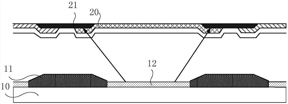
[0049] An embodiment of the present invention provides a display device, such as Figure 4 or Figure 7 As shown, the display device includes a first substrate 01 and a second substrate 02 oppositely arranged, wherein the first substrate 01 is the substrate described in Embodiment 1 or Embodiment 2. The second substrate 02 includes a substrate 10, and a light emitting layer 12 located on the substrate 10 in the sub-pixel region A and a pixel defining layer 11 in the pixel defining region A'. Wherein, the light-emitting layer 12 may include a cathode, an anode, and an organic material light-emitting layer between the cathode and the anode.
[0050] It should be noted that the above-mentioned display device may be a display panel, or may be a display device including a circuit for driving the display panel to display. The present invention is not limited thereto.
[0051] Based on this, combine Figure 4 and Figure 7 , in the display device provided by the embodiment of th...
PUM
 Abstract
Description
Claims
Application Information