Exposure photomask and graphic modeling method of photoresist material

A photoresist material, patterning technology, applied in the field of photoresist material patterning and exposure mask, can solve problems such as poor effect

Inactive Publication Date: 2017-11-21
WUHAN CHINA STAR OPTOELECTRONICS SEMICON DISPLAY TECH CO LTD
View PDF4 Cites 7 Cited by
  • Summary
  • Abstract
  • Description
  • Claims
  • Application Information

AI Technical Summary

Problems solved by technology

However, if the lower film layer under the photoresist structure layer 4 is a heat-sensitive material by using high-temperature baking, the use of high-temperature baking to reduce the slope angle α will be greatly limited.
In addition, by using high-temperature baking, the slope angle α of each position of the entire photoresist structure layer 4 changes accordingly, and it is impossible to only control and reduce the slope angle α of a specified position. However, the slope angle α of some positions α may not need to be reduced or reduced but the effect is not good

Method used


Image

  • Exposure photomask and graphic modeling method of photoresist material
  • Exposure photomask and graphic modeling method of photoresist material
  • Exposure photomask and graphic modeling method of photoresist material

Examples


Embodiment 1

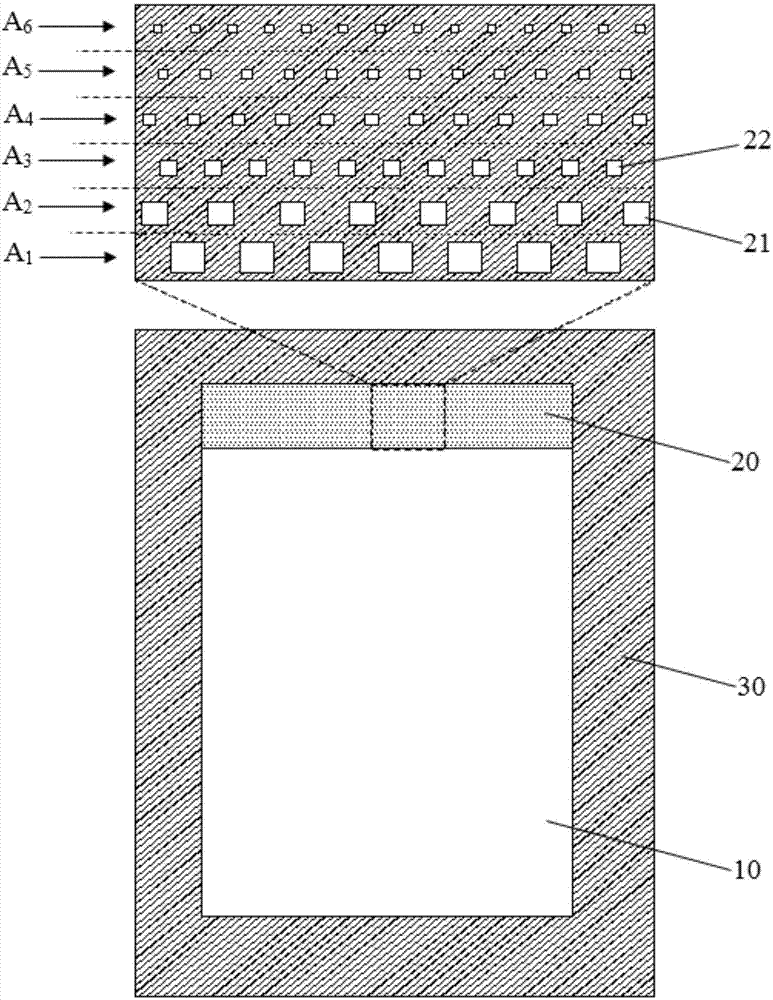
[0032] This embodiment provides an exposure mask, such as image 3 As shown, the exposure mask includes a first exposure area 10, a second exposure area 20 and a light shielding area 30 surrounding the first exposure area 10 and the second exposure area 20, and the second exposure area 20 is adjacent to the The edge of the first exposure area 10 is set. Wherein, the second exposure region 20 includes the first to Mth sub-exposure regions A arranged in parallel in sequence in a direction gradually away from the first exposure region 10 1 ~A M , and, the nth sub-exposure area A n The exposure resolution is greater than the n+1th sub-exposure area A n+1 exposure resolution. Wherein, M is an integer greater than 2, and n=1, 2, 3, . . . , M-1. In this example, if image 3 exemplarily shows 6 sub-exposure areas A 1 ~A 6 , that is, the value of M is 6, and in some other preferred embodiments, the value range of M is preferably 6-10.

[0033] It should be noted that the expos...

Embodiment 2

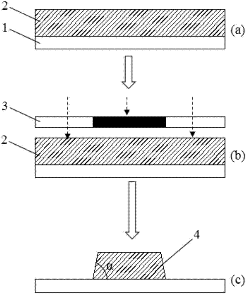
[0040] This embodiment provides a photoresist patterning method, see Figures 4a-4e , the method includes the steps of:

[0041] Step S1, such as Figure 4a As shown, a photoresist material layer 2 is coated on a base substrate 1 .

[0042] Step S2, such as Figure 4b As shown, the first exposure mask 3 is used to expose the photoresist material layer 2 . Wherein, the first exposure mask 3 is a conventional exposure mask in the prior art, and the dotted arrows in the figure indicate exposure light.

[0043] Step S3, such as Figure 4c As shown, the photoresist material layer 2 is developed to form a patterned first photoresist structure layer 4 . The slope angle of the first photoresist structure layer 4 is α 1 .

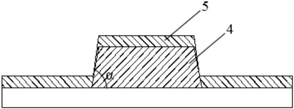
[0044] Step S4, such as Figure 4d As shown, on the first photoresist structure layer 4, a second exposure mask 5 is applied to expose a designated position where the slope angle needs to be adjusted. Specifically, the second exposure mask 5 is the exposure...


PUM


Abstract

The invention discloses an exposure photomask which comprises a first exposure area, a second exposure area and a shading area encircling the first exposure area and the second exposure area, wherein the second exposure area is arranged adjacently to the border of the first exposure area; the second exposure area comprises a first sub-exposure area, ... an M sub-exposure area that are arranged sequentially and in parallel in the direction gradually far away from the first exposure area; the exposure resolution ratio of the n sub-exposure area is greater than that of the (n+1) sub-exposure area; M is an integer which is more than 2; n is equal to 1, 2, 3, ..., M-1. The invention also discloses a graphic modeling method of a photoresist material. Secondary exposure and developing are performed on a graphic photoresist structural layer by the exposure photomask provided by the invention, so that the taper angle of the photoresist structural layer can be changed and adjusted at a specific location.

Description

technical field [0001] The invention belongs to the technical field of displays, relates to an exposure mask, and also relates to a photoresist patterning method using the exposure mask. Background technique [0002] At present, in the process of manufacturing display substrates, an array process is generally used to form a patterned array on the base substrate to obtain a display substrate; there are many types of display substrates, such as common thin-film transistor array substrates, color filter substrates, organic light-emitting diodes, etc. Array substrates or low-temperature polysilicon array substrates, etc. [0003] The display substrate is usually prepared by multiple patterning processes. Each patterning process generally includes the steps of film formation, glue coating, exposure, development, and etching. That is, a layer of substrate film is first formed on the base substrate by the film formation process. Then utilize glue-coating process to coat photoresis...

Claims


Application Information

Patent Timeline
Patent Type & Authority Applications(China)
IPC IPC(8): G03F7/20
CPCG03F7/2022G03F7/70066G03F7/7025
Inventor 李燕
Owner WUHAN CHINA STAR OPTOELECTRONICS SEMICON DISPLAY TECH CO LTD
Why Eureka
Try Eureka