Array substrate and manufacturing method thereof

A technology for array substrates and manufacturing methods, which is applied in semiconductor/solid-state device manufacturing, semiconductor/solid-state device components, instruments, etc., and can solve problems such as poor overlap between the first metal layer and the second metal layer, and large slope angles

Active Publication Date: 2019-05-28
HEFEI XINSHENG OPTOELECTRONICS TECH CO LTD +1
View PDF9 Cites 9 Cited by
  • Summary
  • Abstract
  • Description
  • Claims
  • Application Information

AI Technical Summary

Problems solved by technology

[0005] The present invention provides an array substrate and a manufacturing method thereof, so as to solve the problem of poor overlap between the first metal layer and the second metal layer due to the large slope angle of the connection hole in the existing array substrate manufacturing process

Method used


Image

  • Array substrate and manufacturing method thereof
  • Array substrate and manufacturing method thereof
  • Array substrate and manufacturing method thereof

Examples


Embodiment Construction

[0061] In order to make the above objects, features and advantages of the present invention more comprehensible, the present invention will be further described in detail below in conjunction with the accompanying drawings and specific embodiments.

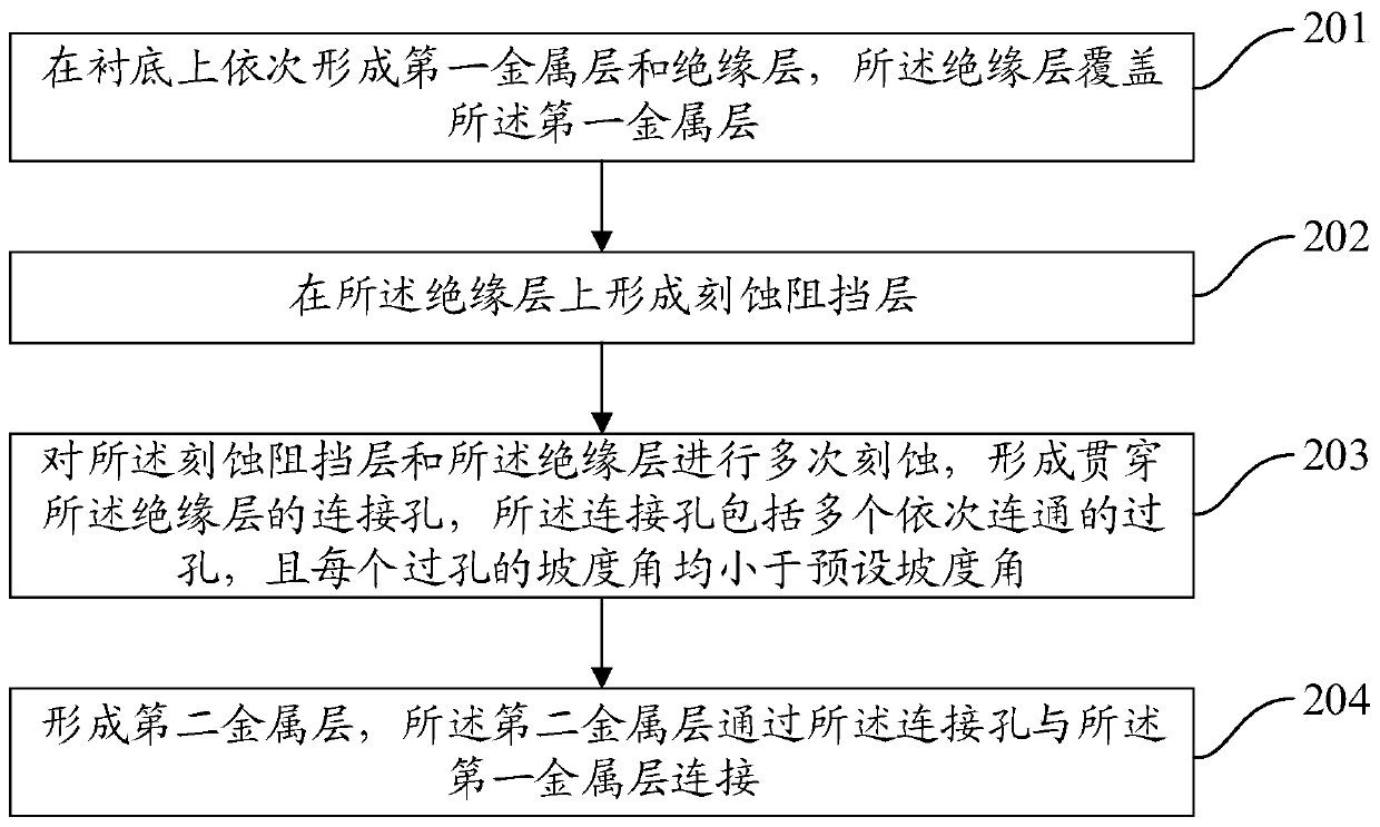
[0062] refer to figure 2 , which shows a flow chart of a method for manufacturing an array substrate according to an embodiment of the present invention, which may specifically include the following steps:

[0063] In step 201, a first metal layer and an insulating layer are sequentially formed on a substrate, and the insulating layer covers the first metal layer.

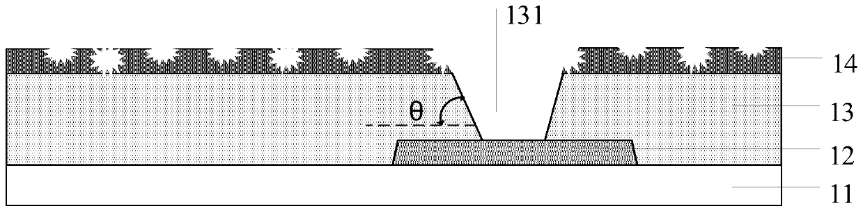
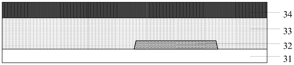
[0064] Such as image 3 As shown, a substrate 31 is first provided, which can be a PI (Polyimide, polyimide) substrate or a glass substrate, and a first metal layer 32 is formed on the substrate 31 by a patterning process, and the patterning process includes a metal thin film Deposition, coating photoresist, mask exposure, development, etching, stripping photoresist...


PUM


Abstract

The invention provides an array substrate and a manufacturing method thereof, and relates to the technical field of display. The manufacturing method comprises the steps of sequentially forming a first metal layer and an insulating layer on a substrate; forming an etching barrier layer on the insulating layer; etching the etching barrier layer and the insulating layer for multiple times to form aconnecting hole penetrating through the insulating layer, wherein the connecting hole comprises a plurality of through holes sequentially communicating with one another, and the slope angle of each through hole is smaller than a preset slope angle; and forming a second metal layer, wherein the second metal layer is connected with the first metal layer through the connecting hole. The etching barrier layer and the insulating layer are etched for multiple times, so that the formed connecting hole comprises a plurality of through holes sequentially communicating with one another; and the thickness of the insulating layer etched each time is small, so that the slope angle of each through hole in the formed connecting hole is smaller than the preset slope angle, poor coverage or broken line ofthe second metal layer caused by the large slope angle of the connecting hole is avoided during subsequent manufacturing of the second metal layer, and poor lap joint of the first metal layer and thesecond metal layer is improved.

Description

technical field [0001] The present invention relates to the field of display technology, in particular to an array substrate and a manufacturing method thereof. Background technique [0002] With the continuous development of display technology, high-precision display technology (such as 8K display technology) has become an important development direction. In high-precision display technology, the wiring method of the array substrate is more dense, and the dense wiring method requires metal wires. The insulating layer between has better connection holes for lapping. [0003] Such as figure 1 As shown, when manufacturing the array substrate, firstly, the first metal layer 12 and the insulating layer 13 are sequentially formed on the substrate 11, and the photoresist 14 is coated on the insulating layer 13, and then the photoresist 14 is exposed and developed. A photoresist hole is formed, and the insulating layer 13 is dry-etched based on the photoresist hole to form a conn...

Claims


Application Information

Patent Timeline
IPC IPC(8): H01L21/48H01L23/498
CPCH01L23/498H01L21/48G02F1/136227H01L27/124H01L27/1248H01L21/76804H01L23/5329G02F1/133345
Inventor 程磊磊方金钢丁录科刘军李伟周斌
Owner HEFEI XINSHENG OPTOELECTRONICS TECH CO LTD
Why Eureka
Try Eureka