
Electronic component

A technology of electronic components and active components, applied in the field of components, can solve problems such as poor product reliability, gas cannot be discharged, peeling, etc., and achieve the effect of reducing the risk of film peeling and improving product yield

Inactive Publication Date: 2017-11-21
AU OPTRONICS CORP
View PDF8 Cites 2 Cited by
  • Summary
  • Abstract
  • Description
  • Claims
  • Application Information

AI Technical Summary

Problems solved by technology

However, in the existing via hole design, undercut may occur due to lateral etching, thereby causing the risk of peeling of the film layer, or the film may be damaged due to under-etching. The gas generated between the layers cannot be discharged, which will cause bubbles between the layers of the film
In this way, it may cause a short circuit or an open circuit, which will eventually lead to low yield and poor product reliability.

Method used


Image

  • Electronic component
  • Electronic component
  • Electronic component

Examples


Embodiment Construction

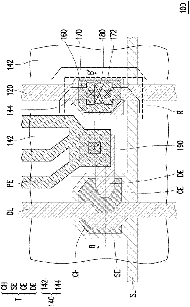
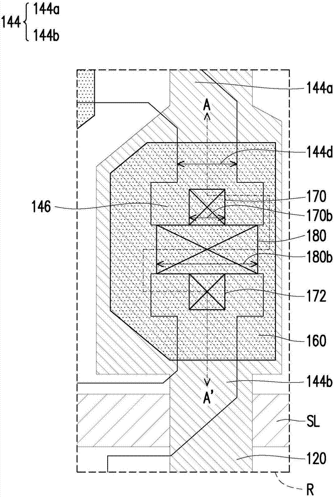
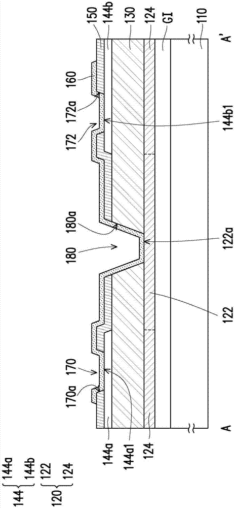
[0070] figure 1 is a schematic top view of an electronic component according to an embodiment of the present invention. figure 2 yes figure 1 Enlarged view of the middle region R. image 3 yes figure 2 The schematic cross-sectional view of the electronic components along the section line A-A'. Figure 4 yes figure 1 The schematic cross-sectional view of the electronic components along the section line B-B'. For clarity and ease of explanation, figure 1 as well as figure 2 Partial film layers are omitted. In the following, the Figure 1 to Figure 4 An embodiment of the present invention will be described in detail.

[0071] Please also refer to Figure 1 to Figure 4 , the electronic component 100 includes a substrate 110 , a signal line 120 , a first insulating layer 130 , a first electrode 140 , a second insulating layer 150 and a second electrode 160 . The signal line 120 is located on the substrate 110 . The first insulating layer 130 is located on the signal ...


PUM


Abstract

An electronic component comprises a substrate, a signal line, a first insulating layer, a first electrode, a second insulating layer and a second electrode. The signal line is arranged on the substrate. The first insulating layer is arranged on the signal line. The first electrode is arranged on the first insulating layer. The second insulating layer is arranged on the first electrode and the first insulating layer. The second electrode is arranged on the second insulating layer. The second insulating layer has a first through hole, and the first insulating layer and the second insulating layer share a second through hole. The signal line is electrically connected with the first electrode by means of the first through hole, the second through hole and the second electrode.

Description

technical field [0001] The present invention relates to a component, and in particular to an electronic component. Background technique [0002] In recent years, in order to achieve more convenience, smaller size and more humanization, many information products have changed from traditional input devices such as keyboards or mice to use touch panels as input devices, which have both touch and display functions. Functional touch display devices have become one of the most popular products today. According to different structures and manufacturing methods, touch display devices can be roughly divided into three types: out-cell, on-cell and in-cell. [0003] During the manufacturing process of the in-cell touch display device, an etching process is required to form through holes. However, in the existing via hole design, undercut may occur due to lateral etching, thereby causing the risk of peeling of the film layer, or the film may be damaged due to under-etching. The gas g...

Claims


Application Information

Patent Timeline
Patent Type & Authority Applications(China)
IPC IPC(8): G06F3/041H01L27/12
CPCG06F3/0412G06F2203/04103H01L27/124H01L27/1244
Inventor 徐文义黄德群陈茂松洪濬成
Owner AU OPTRONICS CORP
Learn More