
Magnetic induction device and manufacturing method therefor

A magnetic induction and device technology, applied in the field of magnetic induction devices and manufacturing, can solve the problems that the performance is easily limited by parasitic capacitance and breakdown voltage, reduce the breakdown voltage of the metal layer, and the breakdown field strength is low, so as to reduce the substrate warpage. buckling and the risk of dielectric peeling, low risk of dielectric peeling, the effect of increasing the breakdown voltage

Active Publication Date: 2017-08-29
成都线易科技有限责任公司 +1
View PDF8 Cites 1 Cited by
  • Summary
  • Abstract
  • Description
  • Claims
  • Application Information

AI Technical Summary

Problems solved by technology

However, low dielectric constant materials are generally loose and porous structures, and the breakdown field strength is low, so the breakdown voltage between metal layers will be reduced
Depositing a thicker dielectric layer can reduce the capacitance and increase the breakdown voltage at the same time, but the process of depositing a thick dielectric layer on a large area of ​​the substrate surface is difficult, and the thick dielectric layer will form a large stress on the substrate, causing the substrate The warpage or even fracture; the dielectric layer itself is also easy to peel off from the substrate under the action of stress
Therefore, using the embedded metal lines in the prior art and the magnetic induction devices formed with the embedded metal lines, the performance is easily limited by parasitic capacitance and breakdown voltage

Method used

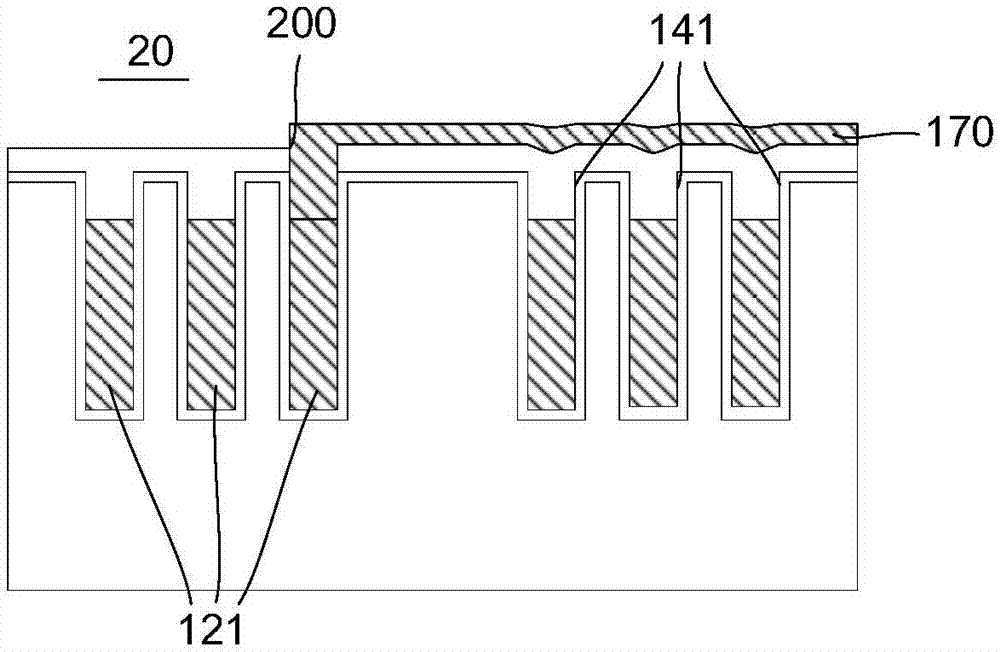
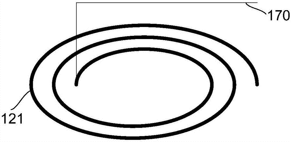

Image

  • Magnetic induction device and manufacturing method therefor
  • Magnetic induction device and manufacturing method therefor
  • Magnetic induction device and manufacturing method therefor

Examples


Embodiment Construction

[0026] The following will clearly and completely describe the technical solutions in the embodiments of the present invention with reference to the accompanying drawings in the embodiments of the present invention. Obviously, the described embodiments are only some, not all, embodiments of the present invention. The following detailed description of the embodiments of the invention provided in the accompanying drawings is not intended to limit the scope of the claimed invention, but merely represents selected embodiments of the invention. Based on the embodiments of the present invention, all other embodiments obtained by those skilled in the art without making creative efforts belong to the protection scope of the present invention.

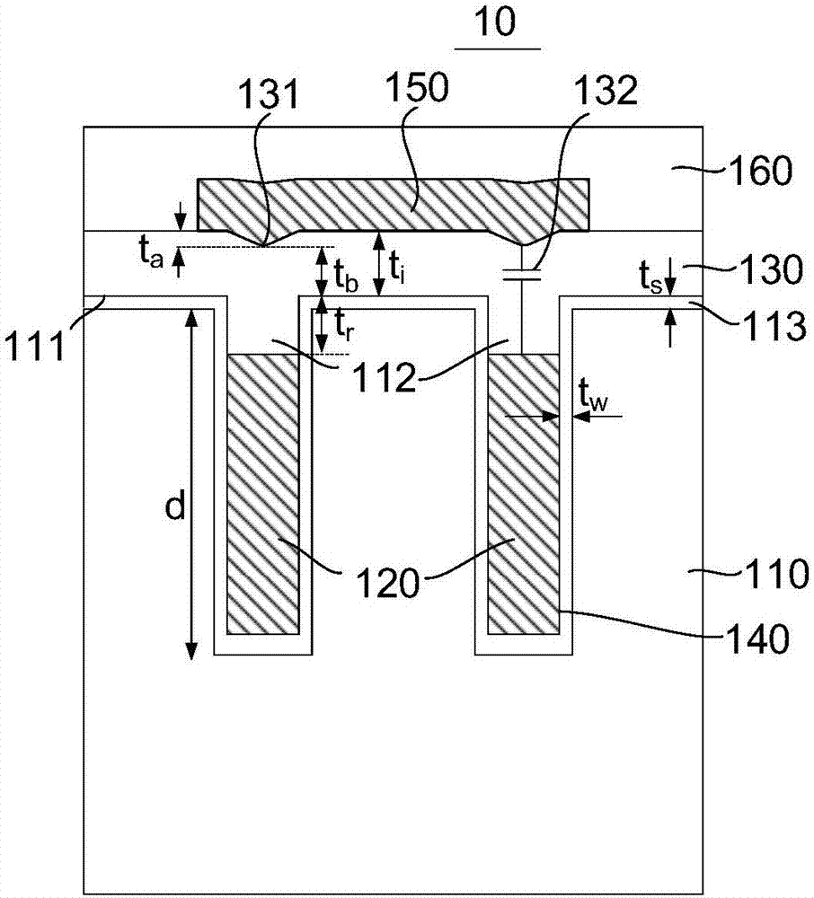
[0027] For details, see figure 1 , figure 1 The magnetic induction device 10 provided by the first embodiment of the present invention is shown, and the magnetic induction device 10 includes a substrate 110 , a first metal layer 120 , a first d...


PUM

PropertyMeasurementUnit
Depthaaaaaaaaaa

Abstract

The invention provides a magnetic induction device. The magnetic induction device comprises a substrate, a first metal layer and a first dielectric layer; a groove is formed in the first surface of the substrate; the first metal layer is arranged in the groove; the surface of the first metal layer is lower than the first surface; the surface of the first metal layer and the first surface form a first concave part; and the first dielectric layer is arranged on the first surface of the substrate and the first concave part is filled with the first dielectric layer. According to the magnetic induction device and the manufacturing method therefor provided by the embodiments, the surface of the first metal layer is lower than the surface of the substrate to form the first concave part; in addition, the first dielectric layer is arranged on the surface of the substrate and the first concave part is filled with the first dielectric layer, so that the thickness of the dielectric between the first metal layer and the surface metal layer is increased while the thickness of the dielectric in other regions is unchanged; and therefore, stray capacitance can be lowered, breakdown voltage can be improved, and risk of substrate warping and dielectric layer stripping also can be lowered.

Description

technical field [0001] The invention relates to the field of electrical components, in particular to a magnetic induction device and a manufacturing method. Background technique [0002] With the development of etching, electroplating, and surface planarization technologies, embedded metal wire technology has been better applied due to its technical advantages of large thickness and low resistance. The embedded metal line technology refers to opening grooves on the surface of the substrate and filling the grooves with metal materials instead of disposing the metal materials on the surface of the substrate. [0003] In the prior art, after the embedded metal lines are formed, the substrate needs to be planarized, so that a surface dielectric layer and a metal layer continue to be formed on the planarized substrate surface. [0004] In order to reduce the parasitic capacitance between the embedded metal wire and the surface metal layer, a low dielectric constant material is u...

Claims


Application Information

Patent Timeline
IPC IPC(8): H01L27/22H01L21/82
CPCH01L21/82H10B61/00H10N59/00
Inventor 方向明伍荣翔单建安
Owner 成都线易科技有限责任公司
Learn More