Circuit board manufacturing method

A manufacturing method and circuit board technology, applied in the direction of multi-layer circuit manufacturing, printed circuit manufacturing, printed circuit, etc., can solve the problems of area utilization rate and wiring density decrease, unfavorable electronic product design, area utilization rate decrease, etc. Area usage, improvement of confinement issues, effect of increasing routing density

Active Publication Date: 2018-02-23
UNIMICRON TECH CORP
View PDF4 Cites 1 Cited by
  • Summary
  • Abstract
  • Description
  • Claims
  • Application Information

AI Technical Summary

Problems solved by technology

In the known circuit board manufacturing method, based on the lithography deviation factor, the annular gasket (annular ring) restricts the width of the contact pad to be larger than the width of the via hole, thereby causing the problem of a decrease in the area utilization rate and making the wiring density affected
figure 1 It is a schematic diagram of the structure of a known circuit board, such as figure 1 As shown, compared with the via hole 120 connected to the conductive layer 110, the width of the pad 130 connected to the circuit layer 140 is larger and cannot be reduced. Therefore, the area utilization rate and the wiring density are reduced, which is not conducive to electronic processing. product design
Furthermore, the known circuit board structure may also have the problem of thin line peeling (peeling)

Method used


Image

  • Circuit board manufacturing method
  • Circuit board manufacturing method
  • Circuit board manufacturing method

Examples


Embodiment Construction

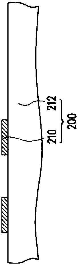
[0043] Figure 2A to Figure 2K It is a schematic cross-sectional view of the manufacturing method of the circuit board according to the first embodiment of the present invention.

[0044] First, please refer to Figure 2A , providing a core layer 200 , wherein the core layer 200 includes a core dielectric layer 212 and a conductive layer 210 on the core dielectric layer 212 . In more detail, the material of the core dielectric layer 212 is, for example, epoxy resin, but not limited thereto. The conductive layer 210 is, for example, a copper layer, and the conductive layer 210 is formed on the core dielectric layer 212 by, for example, lamination. In this embodiment, the core layer 200 may be a double-sided structure or a single-sided structure. For clarity and convenience, Figure 2A to Figure 2K Only a single-panel structure is shown in , but the present invention is not limited thereto.

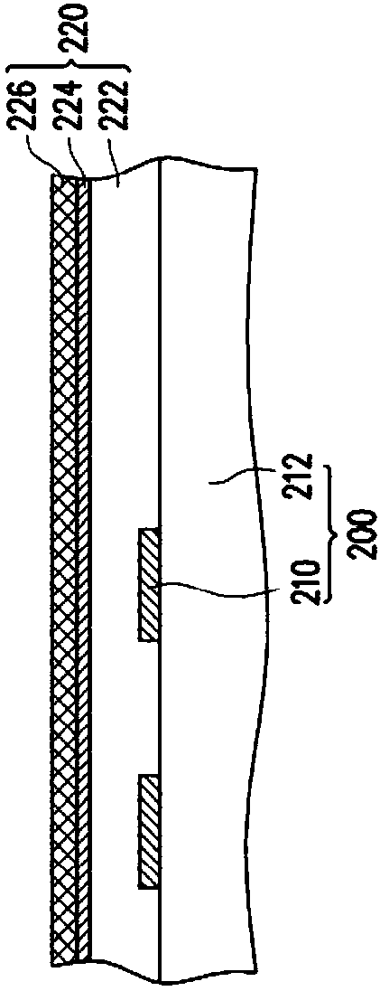
[0045] Next, please refer to Figure 2B , forming a composite material layer 220 ...


PUM


Abstract

The invention provides a circuit board manufacturing method comprising the following steps: placing electronic elements configured with many receive pads into a contain groove formed by jointing a substrate with a bonding layer; forming a dielectric layer so as to cover the receive pads, the electronic elements, the bonding layer and the substrate, and etching the dielectric layer so as to exposethe receive pad top surfaces; forming a composite material layer so as to cover the receive pads and the dielectric layer, wherein the composite material layer comprises a platable dielectric layer, aconductive polymer layer and an anti-plating layer arranged from bottom to top in order; forming a plurality of open holes in the composite material layer so as to expose partial the receive pads andpartial the dielectric layer; forming a metal layer connected with the conductive polymer layer on the open hole bottoms and partial the side wall formed by the platable dielectric layer and the conductive polymer layer; forming a line layer in the open holes, and removing the conductive polymer layer and the anti-plating layer, wherein the line layer top surface is flush with the platable dielectric layer. The method can increase the circuit board area utilization rate and wiring density, and can improve the fine line peeling problems.

Description

technical field [0001] The invention relates to a method for manufacturing a circuit board, in particular to a method for manufacturing a circuit board capable of increasing wiring density. Background technique [0002] In recent years, with the rapid development of electronic technology, more user-friendly technology products have come out one after another. At the same time, these technology products are designed towards the trend of light, thin, short and small. In the known circuit board manufacturing method, based on the lithography deviation factor, the annular gasket (annular ring) restricts the width of the contact pad to be larger than the width of the via hole, thereby causing the problem of a decrease in the area utilization rate and making the wiring density affected. figure 1 It is a schematic diagram of the structure of a known circuit board, such as figure 1 As shown, compared with the via hole 120 connected to the conductive layer 110, the width of the pad ...

Claims


Application Information

Patent Timeline
Patent Type & Authority Applications(China)
IPC IPC(8): H05K3/46
CPCH05K3/4644H05K2203/072H05K2203/0723
Inventor 林建辰
Owner UNIMICRON TECH CORP
Why Eureka
Try Eureka