
Window type ball grid array packaging module

A ball grid array and packaging component technology, which is applied in the field of semiconductor storage components, can solve the problems of external failure of the package, high mold flow pressure, deformation and sinking, etc.

Inactive Publication Date: 2017-11-21
RUILI INTEGRATED CIRCUIT CO LTD
View PDF5 Cites 3 Cited by
  • Summary
  • Abstract
  • Description
  • Claims
  • Application Information

AI Technical Summary

Problems solved by technology

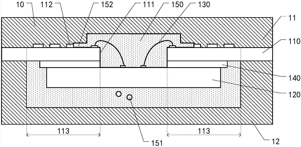
At the same time, due to the different velocity of the upper and lower mold flow, when the upper mold flow is greater than the lower mold flow, the mold flow pressure above the substrate 110 will be high, and the unclamped area 113 of the substrate 110 will deform and sink. When the molding compound flows to the glue outlet 111B, because the flow rate is too fast, it will increase the pressure of the upper mold flow to open the substrate 110, causing the molding compound to overflow from the gap between the upper mold cavity and the substrate 110 to the substrate 110 to produce overflowing glue 152, and the overflowing glue 152 will even cover the solder joint. disc 112, which disables the package’s external
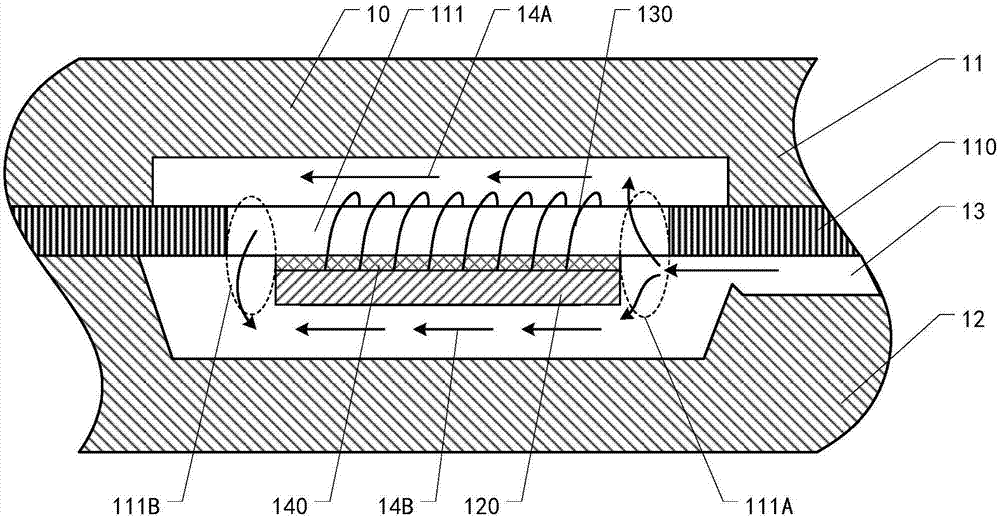
like image 3 As shown, if the chip 120 is displaced in the direction opposite to the glue inlet 111A', the area of ​​the glue outlet 111B' will become narrower than the area of ​​the glue inlet 111A', and the problems of voids and glue overflow will become smaller. more serious

Method used


Image

  • Window type ball grid array packaging module
  • Window type ball grid array packaging module
  • Window type ball grid array packaging module

Examples


Embodiment Construction

[0043] In the following, only some exemplary embodiments are briefly described. As those skilled in the art would realize, the described embodiments may be modified in various different ways, all without departing from the spirit or scope of the present invention. Accordingly, the drawings and descriptions are to be regarded as illustrative in nature and not restrictive.

[0044] Such as Figure 4 , Figure 5 and Figure 6 As shown, the window type ball grid array package assembly of this embodiment includes a substrate 210 , a chip 220 , bonding wires 230 , an adhesive layer 240 , a plastic package 250 and solder balls 260 .

[0045] The substrate 210 has a first surface 212 and a second surface 213 opposite to each other, and a window 211 penetrating through the first surface 212 and the second surface 213 is formed. A plurality of contacts 215 adjacent to the window 211 and a plurality of bonding pads 216 arranged in a matrix are disposed on the first surface 212 of the...


PUM


Abstract

The invention provides a window type ball grid array packaging module. The window type ball grid array packaging module comprises a substrate, which includes a first surface and a second surface which are opposite to each other, and a window penetrating through the first surface and the second surface is formed on the substrate, wherein the first surface is provided with a plurality of contacts adjacent to the window and a plurality of bonding pads in matrix arrangement; the second surface includes a chip installation area, and a glue inlet through which a glue is entered and a glue outlet through which the glue is discharged during injection molding are formed at the two ends of the window respectively, wherein the glue inlet and the glue outlet exceed the chip installation area; the glue outlet is a slow opening with an enlarged size compared with the glue inlet, and the end width of the glue outlet is greater than the channel width of the window; a chip, which partially covers the window, and makes the glue inlet and the glue outlet of the window exposed to the outside of the chip; a bonding wire, which penetrates through the window and is electrically connected with the chip and the substrate; and a plastic package body, which packages the chip and the bonding wire, and fills the glue outlet. The window type ball grid array packaging module provided by the invention can avoid the problem of glue overflow on the substrate and cavities appearing in the plastic package body due to too fast mold flow velocity in an upper mold in the injection molding process.

Description

technical field [0001] The present invention relates to semiconductor storage components, in particular to a window ball grid array (Window Ball Grid Array, WBGA) packaging component. Background technique [0002] Among the package types of semiconductor devices, the window type ball grid array package structure is to open a through window for the substrate carrying the chip, so that the bonding wire can pass through the window and electrically connect the substrate and the chip. [0003] Such as figure 1 As shown, a known window-type ball grid array package includes a substrate 110 with a window 111, a chip 120, a bonding wire 130, an adhesive layer 140, a plastic package 150, and solder balls, and the solder balls are planted on the joint of the substrate 110. pad 112 on the surface. The chip 120 is fixed on the mounting surface of the substrate 110 through the adhesive layer 140 , the bonding wire 130 passes through the window 111 to electrically connect the chip 120 an...

Claims


Application Information

Patent Timeline
IPC IPC(8): H01L23/31H01L23/498
CPCH01L23/49816H01L23/31H01L23/3128H01L23/488H01L2924/181H01L2224/05553H01L2224/32225H01L2224/48091H01L2224/4824H01L2224/73215H01L2924/00014H01L2924/00012H01L2924/00
Inventor 庄凌艺
Owner RUILI INTEGRATED CIRCUIT CO LTD
Learn More