Low-noise reading circuit for CMOS image sensor and reading method thereof

An image sensor and readout circuit technology, applied in the field of image sensors, can solve the problems of poor image quality, failure to improve image quality, and signal submersion in noise, so as to improve image quality, be suitable for popularization and use, and reduce equivalent Effect of Input Noise

Active Publication Date: 2017-11-24
SHANGHAI INTEGRATED CIRCUIT RES & DEV CENT +1
View PDF6 Cites 1 Cited by
  • Summary
  • Abstract
  • Description
  • Claims
  • Application Information

AI Technical Summary

Problems solved by technology

Especially in low-light conditions, due to the relatively small photo-generated current, the signal is easily submerged in noise, and the image quality is particularly poor in low-light environments.
[0003] The method used for noise processing in the prior art is CDS technology, that is, correlated double sampling technology. This method is widely used in the field of CMOS image sensors. This technology can reduce the FPN of the pixel unit and the noise of the source follower. The effect is limited in the environment, and the image quality problem in the low-light environment cannot be improved.

Method used


Image

  • Low-noise reading circuit for CMOS image sensor and reading method thereof
  • Low-noise reading circuit for CMOS image sensor and reading method thereof
  • Low-noise reading circuit for CMOS image sensor and reading method thereof

Examples


Embodiment 1

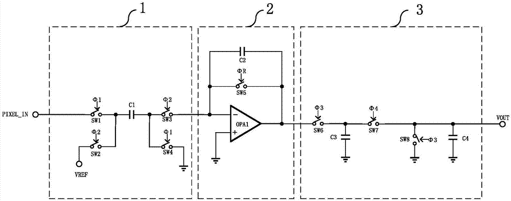
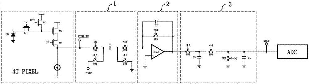
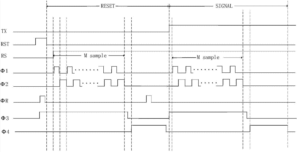
[0039] Such as figure 2 , image 3 As shown, the readout circuit proposed by the present invention is connected to the standard 4T PIXEL, and the MOS transistors connected to the photodiode are M1, M2, M3 and M4, wherein, the TX signal is applied to M1, the RST signal is applied to M2, and the M4 is applied to RS signal, add Φ1 signal to SW1 and SW4, add Φ2 signal to SW2 and SW3, add ΦR signal to SW5, add Φ3 signal to SW6 and SW8, and add Φ4 signal to SW7. The specific readout method steps are as follows:

[0040] Step 1: After the photodiode PD is exposed, RST changes from low level to high level, and then from high level to low level again. During this time interval, ΦR appears a high pulse, and then keeps low level. Φ3 changes from low level to high level, so that the sixth switch SW6 and the eighth switch SW8 are turned on.

[0041] Step 2: RS changes from low level to high level, and the RESET signal is output through the source of M4.

[0042] Step 3: The control sig...


PUM


Abstract

The invention discloses a low-noise reading circuit for a CMOS image sensor and a reading method thereof. The reading circuit comprises a signal multiple-sampling module, a signal integration module and a signal averaging module. Two ends of the signal integration module are connected with the signal multiple-sampling module and the signal averaging module. The other end of the signal integration module is a signal input end. The other end of the signal averaging module is a signal output end. The signal multiple-sampling module carries out multiple-sampling processing on to-be-processed signals and transmits the signals to the signal integration module for integration summation; the integration summation signals are transmitted to the signal averaging module for averaging; and an average signal is output through the signal output end. According to the low-noise reading circuit for the CMOS image sensor provided by the invention, the PIXEL equivalent input noises can be effectively reduced, the low-noise reading circuit is particularly applicable to a low light environment; the image quality can be effectively improved; and the low-noise reading circuit is suitable for popularized usage.

Description

technical field [0001] The invention relates to the field of image sensors, in particular to a low-noise readout circuit of a CMOS image sensor and a readout method thereof. Background technique [0002] In the field of image sensors, improving image quality is an eternal theme. The photosensitive signal of the image sensor will be affected by various noise sources during transmission, making it difficult to improve the signal-to-noise ratio. Noise can cause various FPN (solid state noise) and various random bright or dark spots in the image. Especially in low-light conditions, because the photogenerated current is relatively small, the signal is easily submerged in noise, and the image quality is particularly poor in low-light environments. [0003] The method used for noise processing in the prior art is CDS technology, that is, correlated double sampling technology. This method is widely used in the field of CMOS image sensors. This technology can reduce the FPN of the ...

Claims


Application Information

Patent Timeline
Patent Type & Authority Applications(China)
IPC IPC(8): H04N5/374H04N5/357H04N5/378
CPCH04N25/60H04N25/76H04N25/75
Inventor 段杰斌温建新李琛皮常明蒋宇
Owner SHANGHAI INTEGRATED CIRCUIT RES & DEV CENT
Why Eureka
Try Eureka