Transparent display panel and manufacturing method thereof and display system

A transparent display panel and transparent substrate technology, applied in the direction of instruments, nonlinear optics, optics, etc., to achieve the effect of improving uniformity and reducing the influence of transmittance

Inactive Publication Date: 2017-12-01
BOE TECH GRP CO LTD
View PDF15 Cites 14 Cited by
  • Summary
  • Abstract
  • Description
  • Claims
  • Application Information

AI Technical Summary

Problems solved by technology

[0005] The object of the present invention is to provide a transparent display panel, its manufacturing method and display system to solve the problem of how to improve the transmittance and display uniformity of the transparent display device

Method used


Image

  • Transparent display panel and manufacturing method thereof and display system
  • Transparent display panel and manufacturing method thereof and display system
  • Transparent display panel and manufacturing method thereof and display system

Examples


Embodiment Construction

[0038] The following will clearly and completely describe the technical solutions in the embodiments of the present invention with reference to the accompanying drawings in the embodiments of the present invention. Obviously, the described embodiments are only some, not all, embodiments of the present invention. Based on the embodiments of the present invention, all other embodiments obtained by persons of ordinary skill in the art without making creative efforts belong to the protection scope of the present invention.

[0039] Wherein, the thickness of the film layer and the shape of the area in the drawings do not reflect the real scale, and the purpose is only to illustrate the content of the present invention.

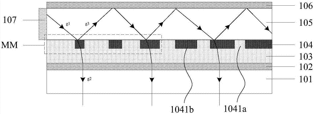
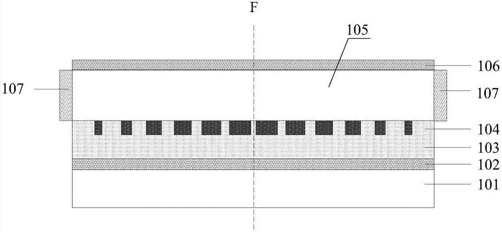
[0040] Such as figure 1 As shown, it is a schematic cross-sectional structure diagram of a transparent display panel provided by an embodiment of the present invention; the transparent display panel includes: a transparent substrate 101, and a first electrode layer...


PUM


Abstract

The invention relates to a transparent display panel and a manufacturing method thereof and a display system with an aim to the problem about improving transmittance and display uniformity of a display device. The transparent display panel comprises a transparent substrate and a first electrode layer, a liquid crystal layer, a transmission film layer, an optical waveguide layer and a second electrode layer which are sequentially arranged on the transparent substrate, and at least one light source arranged on the side face of the optical waveguide layer; the transmission film layer includes multiple opening zones partitioning the transmission film layer into multiple independent sub-transmission films; the width of the opening zones are decreased sequentially from locations of the light sources to opposite-side directions of the light sources, and the width of the sub-transmission films are sequentially increased from locations of the light sources to the opposite-side directions of the light sources; refractive index of the sub-transmission films is not less than that of the optical waveguide layer; the refractive index of each of the sub-transmission films, the liquid crystal layer and the transparent substrate is increased sequentially; poor display uniformity caused by optical propagation loss can be reduced, and display uniformity of the display panel is improved.

Description

technical field [0001] The invention relates to the technical field of transparent display, in particular to a transparent display panel, a manufacturing method thereof and a display system. Background technique [0002] With the development of display technology, and the increasing demand for the use of portable information media, in recent years, so-called transparent display devices, which can see the displayed information and display on the display screen when a voltage is applied, have been actively researched and developed. objects behind the screen, and objects behind the display can be seen through the display like glass when no voltage is applied. [0003] In the structure of the existing transparent display device, some schemes need to attach a scattering film on the glass as a transparent glass screen, and cooperate with the projection equipment to project the picture to be displayed onto the glass screen. Although the production process of this scheme is simple, ...

Claims


Application Information

Patent Timeline
Patent Type & Authority Applications(China)
IPC IPC(8): G02F1/13357G02F1/1335G02F1/1333
CPCG02F1/1333G02F1/1335G02F1/133615
Inventor 魏伟
Owner BOE TECH GRP CO LTD
Why Eureka
Try Eureka