Thin film transistor and array substrate
A technology of thin film transistors and array substrates, applied in the display field, can solve the problems of reducing the transmittance of a single board, and achieve the effect of improving the transmittance of a single board and reducing the impact.
- Summary
- Abstract
- Description
- Claims
- Application Information
AI Technical Summary
Problems solved by technology
Method used
Image

Examples
Embodiment 1
[0031] Example 1. Thin Film Transistor
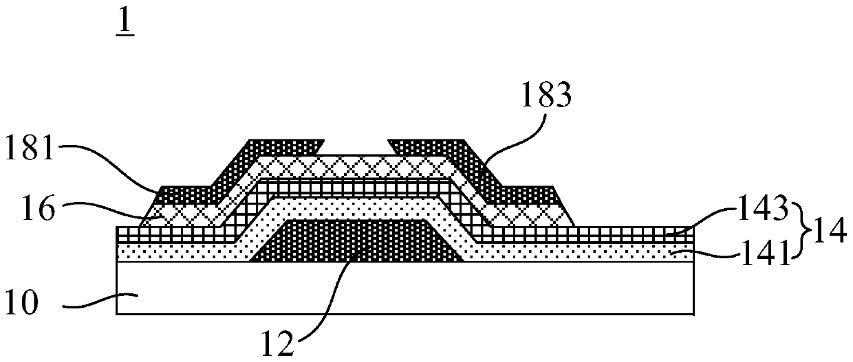
[0032] In this embodiment, a thin film transistor 1 is provided, such as figure 2 As shown, the thin film transistor 1 is formed on a film-forming substrate 10, and includes: a gate 12 disposed on the film-forming substrate 10, a gate insulating layer 14 covering the gate 12, and disposed on the film-forming substrate 10. The semiconductor active layer 16 on the gate insulating layer 14 , and the source electrode 181 and the drain electrode 183 disposed on the semiconductor active layer 16 . The material of the semiconductor active layer 16 is indium gallium zinc oxide (IGZO).
[0033] Such as figure 2 As shown, the gate insulating layer 14 includes: a first gate insulating layer 141 covering the gate 12 , and a second gate insulating layer 143 disposed on the first gate insulating layer 141 . The thickness of the gate insulating layer 14 is less than or equal to 700 nm, and the thickness of the first gate insulating layer 141 is 8...
Embodiment 2
[0040] Example 2. Thin Film Transistor
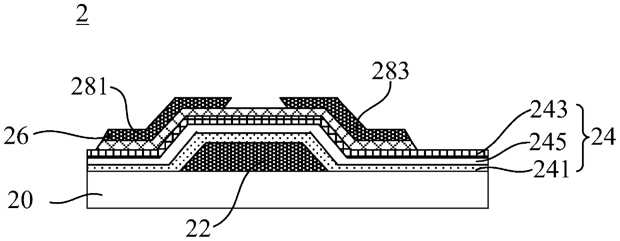
[0041] In this embodiment, a thin film transistor 2 is provided, such as Figure 3A and Figure 3B As shown, the thin film transistor 2 is formed on a film-forming substrate 20, and includes: a gate 22 disposed on the film-forming substrate 20, a gate insulating layer 24 covering the gate 22, and disposed on the film-forming substrate 20. The semiconductor active layer 26 on the gate insulating layer 24 , and the source electrode 281 and the drain electrode 283 disposed on the semiconductor active layer 26 .
[0042] Different from the thin film transistor 1 in Embodiment 1, the gate insulating layer 24 of the thin film transistor 2 in this embodiment includes a first gate insulating layer 241, a second gate insulating layer 243 and a third gate insulating layer 245 . In this embodiment, the third gate insulating layer 245 may be as Figure 3A The shown arrangement is between the first gate insulating layer 241 and the second gate i...
Embodiment 3
[0046] Example 3. Array substrate
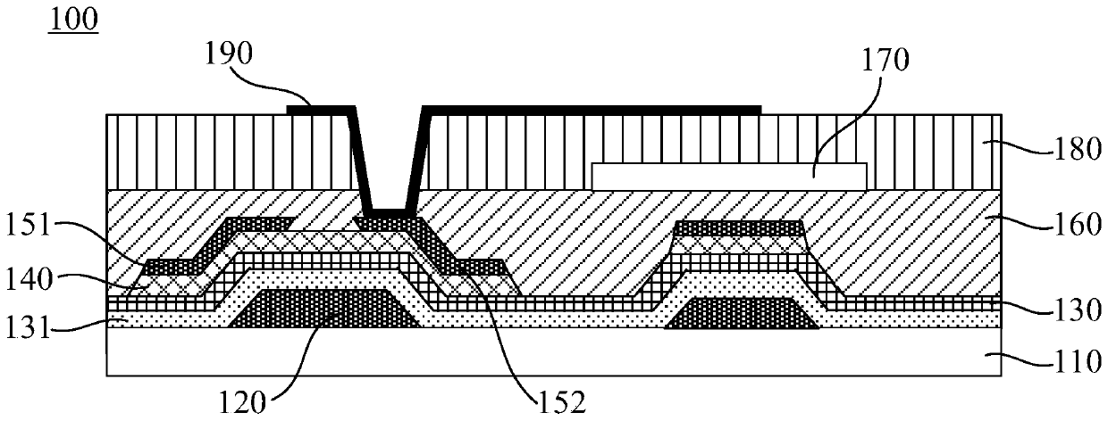
[0047] In this embodiment, an array substrate 3 is provided, and the array substrate 3 includes a plurality of thin film transistors arranged in an array. Figure 4 Described is the thin film transistor structure in a pixel unit on the array substrate 3 . As an example, Figure 4 The array substrate 3 shown in the figure includes: a base substrate 30, a thin film transistor 1 disposed on the base substrate 30, a first passivation layer 32 covering the thin film transistor 1, disposed on the first A color resist layer 34 on a passivation layer, a second passivation layer 36 disposed on the color resist layer 34 , and a pixel electrode 38 disposed on the second passivation layer 36 . Such as Figure 4 As shown, the pixel electrode 38 is connected to the drain electrode 183 of the thin film transistor 1 through the first passivation layer 32 and the second passivation layer 36 .
[0048] Those skilled in the art can understand that the arra...
PUM
 Abstract
Description
Claims
Application Information