OLED package and packaging method thereof

a technology of organic light-emitting diodes and packaging methods, which is applied in the direction of thermoelectric device junction materials, semiconductor devices, electrical apparatus, etc., can solve the problems of not being applied to the top emission type oled devices, reducing service life, etc., to reduce the number of stacked layers, reduce the thickness of the package, and improve the optical

Active Publication Date: 2013-09-19
HANNSTAR DISPLAY CORPORATION
View PDF9 Cites 38 Cited by
  • Summary
  • Abstract
  • Description
  • Claims
  • Application Information

AI Technical Summary

Benefits of technology

[0010]It is an object of the present disclosure to provide an OLED package and a packaging method thereof that can reduce the number of st...

Problems solved by technology

However, the OLED device can be easily damaged by the invasion of moisture and oxygen to decrease the service life.
However in this structure, as the metal cover 73 is opaque to light, it can not be applied to the top emission type OLED device.
In addition, the sealant 74 further has the problem of unable to block moisture effectively.
However, in this structure the glass thickness is difficult to be reduced and the manufacturing stability of the glass cement 84 is not good enough to be ...

Method used


Image

  • OLED package and packaging method thereof
  • OLED package and packaging method thereof
  • OLED package and packaging method thereof

Examples


first embodiment

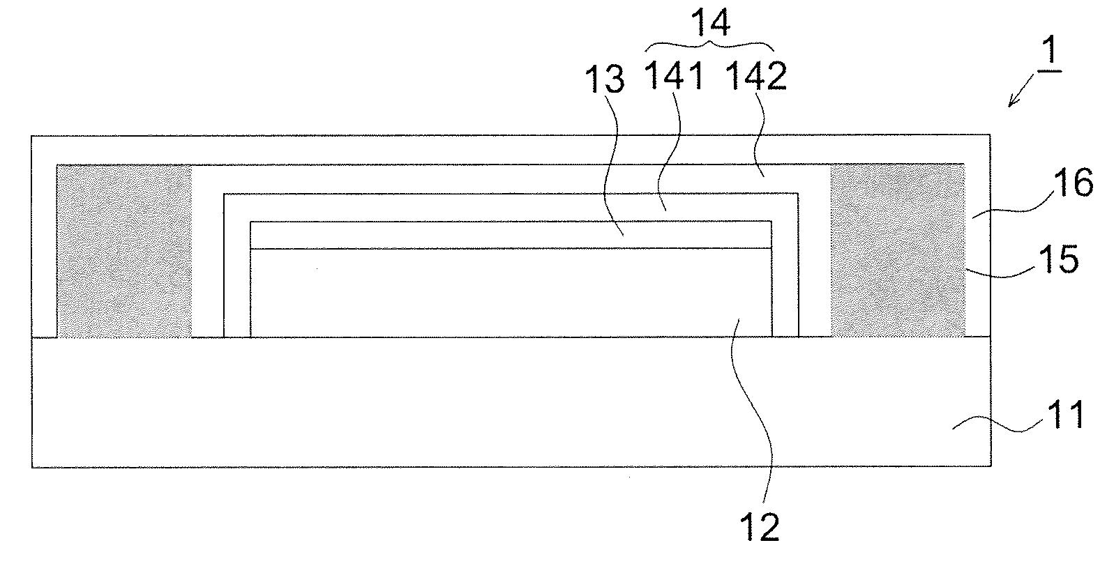
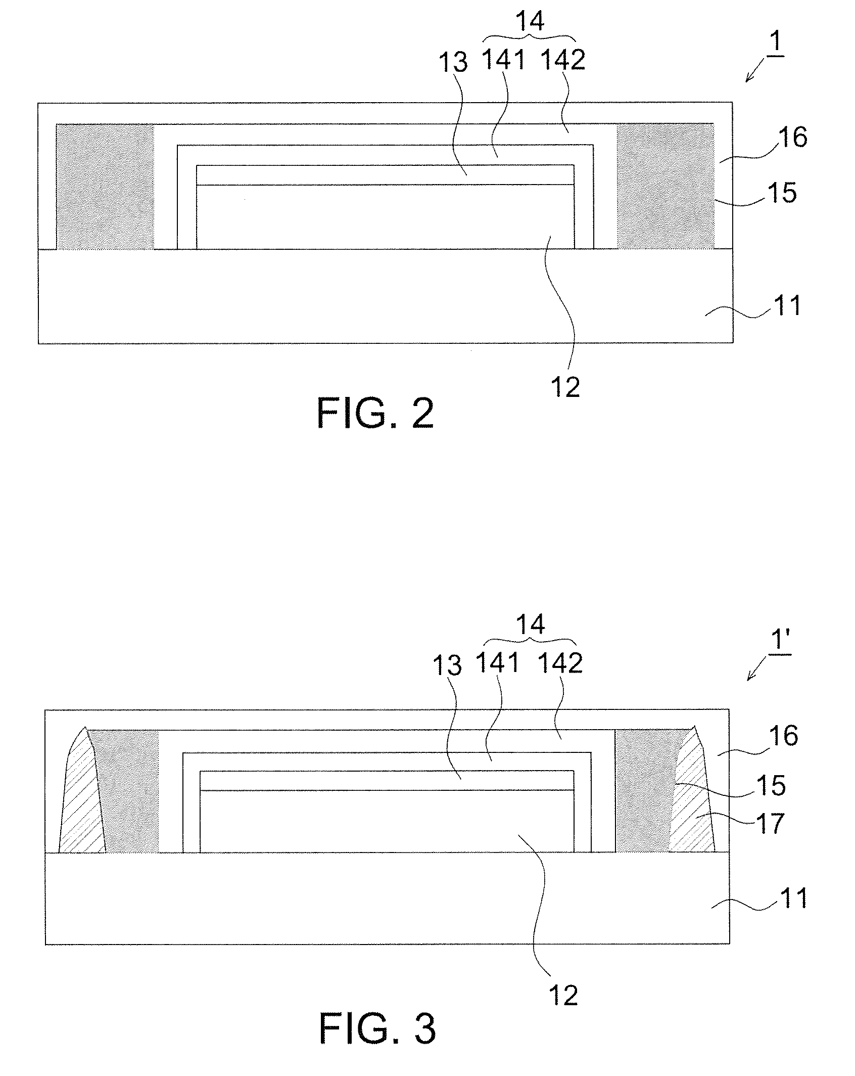
[0028]Referring to FIG. 2, it shows a schematic diagram of the organic light emitting diode (OLED) package according to the present disclosure. The OLED package 1 includes a substrate 11, a lighting component 12, an organic buffer layer 13, a compound barrier layer 14, a moisture absorption zone 15 and an inorganic barrier layer 16.

[0029]The lighting component 12 is an OLED device and formed on the substrate 11. It is appreciated that the lighting component 12 generally has two electrodes (i.e. anode and cathode) and an organic emitting layer sandwiched between the two electrodes. The two electrodes and the organic emitting layer are sequentially formed on the substrate 11 by, for example vapor deposition or coating, wherein the structure and the manufacturing method of the lighting component 12 are well known to the art and thus details thereof are not described herein.

[0030]The organic buffer layer 13 may be a metal complex such as NPB or CuPc which is directly formed on an upper ...

second embodiment

[0036]Similarly, in the second embodiment when moisture outside the OLED package 1′ passes though the inorganic barrier layer 16 to enter the compound barrier layer 14 (more specifically the organic film layer 142), the invaded moisture will follow possible paths in the compound barrier layer 14 to be absorbed by the moisture absorption zone 14 and does not further invade into the lighting component 12. Therefore, the service life can be effectively extended and the total thickness of the package structure will not be increased.

[0037]FIGS. 4A to 4C show schematic diagrams of the packaging method of the OLED package 1 according to the first embodiment of the present disclosure; and FIG. 5 shows a flow chart of the packaging method of the OLED package 1 according to the first embodiment of the present disclosure including the following steps.

[0038]As shown in FIG. 4A, at first a substrate 11 is provided (Step S21). Then a lighting component 12 is formed on the substrate 11 (Step S22),...


PUM


Abstract

There is provided an OLED package including a substrate, a lighting component, a compound barrier layer, a moisture absorption zone and an inorganic barrier layer. The lighting component is formed on the substrate. The compound barrier layer completely seals the lighting component configured to block moisture and oxygen. The moisture absorption zone is formed on the substrate surrounding the compound barrier layer and is not formed upon the lighting component. The inorganic barrier layer completely seals the compound barrier layer and the moisture absorption zone configured to block moisture and oxygen.

Description

CROSS REFERENCE TO RELATED APPLICATION[0001]This application claims the priority benefit of Chinese Patent Application Number 201210088176.8, filed on Mar. 19, 2012, the full disclosure of which is incorporated herein by reference.BACKGROUND[0002]1. Field of the Disclosure[0003]This disclosure generally relates to an organic light emitting diode (OLED) structure and, more particularly, to an OLED package and a packaging method thereof.[0004]2. Description of the Related Art[0005]As the organic light emitting diode display (OLED display) has the superiority of high color saturation, high brightness and wide viewing angle, it becomes a popular product in the next generation display market. However, the OLED device can be easily damaged by the invasion of moisture and oxygen to decrease the service life. Therefore, how to prevent moisture and oxygen from invading into the OLED device is an important research topic in this field.[0006]FIG. 1A shows a conventional OLED package which incl...

Claims


Application Information

Patent Timeline
IPC IPC(8): H01L51/52H01L51/56H01L33/52
CPCH01L51/52H01L33/52H01L51/5259H01L51/5256H01L51/56H10K50/846H10K50/8445H10K50/80H10K71/00
Inventor LIN, CHIH-PIN
Owner HANNSTAR DISPLAY CORPORATION
Why Eureka
Try Eureka