Array substrate and display panel

A technology for array substrates and display panels, applied in static indicators, nonlinear optics, instruments, etc., can solve the problems of unfavorable narrow frame design of displays, save external lead bonding area, reduce width, enhance connection strength and conductivity The effect of efficiency

Active Publication Date: 2017-12-01
SHENZHEN CHINA STAR OPTOELECTRONICS TECH CO LTD
View PDF6 Cites 24 Cited by
  • Summary
  • Abstract
  • Description
  • Claims
  • Application Information

AI Technical Summary

Problems solved by technology

[0003] The technical problem mainly solved by the present invention is to provide an array substrate and a display panel, which can solve the problem that the display in the prior art is not conducive to the realization of a narrow frame design

Method used


Image

  • Array substrate and display panel
  • Array substrate and display panel
  • Array substrate and display panel

Examples


no. 1 example

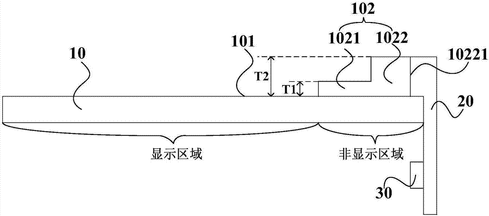
[0016] Such as figure 1 As shown, the first embodiment of the array substrate of the present invention includes:

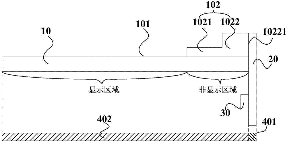
[0017] The substrate 10, relative to the pad 102 fixed on the non-display area of ​​the first surface 101 of the substrate 10, the pad 102 includes a first area 1021 and a second area 1022, the thickness T1 of the first area 1021 is smaller than the thickness T2 of the second area 1022, The second area 1022 is used for connecting the flexible circuit board 20 ; wherein, the first area 1021 is closer to the display area of ​​the substrate 10 than the second area 1022 .

[0018] Specifically, the substrate 10 is an array substrate, and the array substrate is prepared with an array layer of thin film transistors (ThinFilm Transistor, TFT for short), the substrate 10 can be a glass substrate or a flexible substrate, and the pad 102 is relatively fixed on the substrate 10 A non-display area of ​​the surface 101, the pad 102 includes a first area 1021 and a second area...

1 example 80

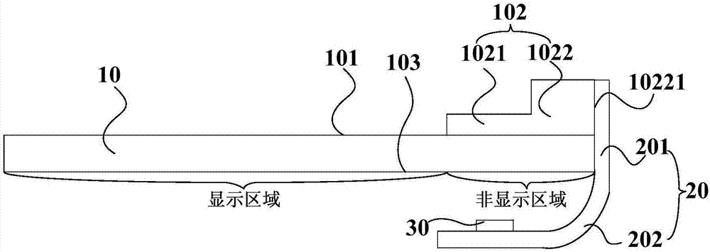
[0034] Further, an embodiment 80 of the display panel of the present invention also includes:

[0035] The driving chip 806 is disposed on the flexible circuit board 805 , the encapsulation layer 807 is disposed on a surface 8012 of the pad 8011 away from the array substrate 801 , and the light-shielding resin 808 is coated on the edge of the display panel 80 .

[0036]Wherein, the driving chip 806 is a chip for driving the TFT circuit in the array substrate 801 , and the encapsulation layer 807 is a sealant frame around the display area of ​​the display panel 80 .

[0037] In this embodiment, the pad of the non-display area of ​​the array substrate of the display panel includes a first area and a second area, the thickness of the first area is smaller than the thickness of the second area, and the second area is used to connect the flexible circuit board ; Wherein, the first area is closer to the display area of ​​the substrate than the second area, the flexible circuit board...


PUM

PropertyMeasurementUnit
thicknessaaaaaaaaaa
thicknessaaaaaaaaaa

Abstract

The invention discloses an array substrate and a display panel. The array substrate comprises a substrate body and a bonding pad relatively fixed to a nondisplay area of one surface of the substrate body, the bonding pad comprises a first area and a second area, the thickness of the first area is smaller than that of the second area, and the second area is used for connecting a flexible circuit board; the first area is closer to a display area compared with the second area, the flexible circuit board is relatively fixed to one surface of the second area, and the surface of the second area is perpendicular to the surface of the substrate. In this way, the width of nondisplay area can be decreased, and narrow frame design is achieved conveniently.

Description

technical field [0001] The present invention relates to the field of display technology, in particular to an array substrate and a display panel. Background technique [0002] The display has a display area formed by an array of display pixels and a non-display area surrounding the display area. The non-display area includes support circuits such as signal lines, driver circuits, and bond pads, but does not include active pixels used to generate images. In the prior art, in the non-display area, the flexible circuit board carrying the driver chip is usually placed directly on the bonding pad to form an external wire bonding area. Therefore, the existence of the external wire bonding area of ​​the display is not conducive to realizing a narrow frame design. Contents of the invention [0003] The technical problem mainly solved by the present invention is to provide an array substrate and a display panel, which can solve the problem that the display in the prior art is not ...

Claims


Application Information

Patent Timeline
Patent Type & Authority Applications(China)
IPC IPC(8): G02F1/1345G02F1/133
CPCG02F1/13306G02F1/13458
Inventor 阙成文
Owner SHENZHEN CHINA STAR OPTOELECTRONICS TECH CO LTD
Why Eureka
Try Eureka