Eureka AIR delivers breakthrough ideas for toughest innovation challenges, trusted by R&D personnel around the world.

Display substrate, manufacturing method thereof and display panel

A display substrate and display panel technology, which is applied in semiconductor/solid-state device manufacturing, instruments, semiconductor devices, etc., can solve the problems of poor display effect of display panels, improve display effect, prevent influence, and improve the effect of ink mura

Active Publication Date: 2017-12-12
BOE TECH GRP CO LTD +1
View PDF15 Cites 1 Cited by
  • Summary
  • Abstract
  • Description
  • Claims
  • Application Information

AI Technical Summary

Problems solved by technology

[0005] The present invention provides a display substrate, a manufacturing method thereof, and a display panel, which can solve the problem that in the prior art, when an external electric field exists around the display panel, the display area of ​​the display panel will be affected by the external electric field, resulting in poor display effect of the display panel. Poor problem, the technical solution is as follows:

Method used


Image

  • Display substrate, manufacturing method thereof and display panel
  • Display substrate, manufacturing method thereof and display panel
  • Display substrate, manufacturing method thereof and display panel

Examples


Embodiment Construction

[0044] In order to make the purpose, technical solutions and advantages of the present disclosure clearer, the present disclosure will be further described in detail below in conjunction with the accompanying drawings. Obviously, the described embodiments are only some of the embodiments of the present disclosure, not all of them. . Based on the embodiments in the present disclosure, all other embodiments obtained by persons of ordinary skill in the art without creative efforts fall within the protection scope of the present disclosure.

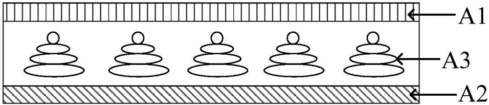
[0045] With the development of display technologies, there are more and more types of display panels. For example, the display panels may include liquid crystal display panels and organic light-emitting diode (English: Organic Light-Emitting Diode; abbreviated: OLED) display panels. example, figure 1 It is a structural schematic diagram of a traditional liquid crystal display panel, such as figure 1 As shown, the liquid crystal display pane...


PUM


Abstract

The invention provides a display substrate, a manufacturing method thereof and a display panel, and belongs to the technical field of display. The display substrate comprises an underlayer substrate, a BM (black matrix) is arranged on the underlayer substrate, the underlayer substrate has a display area and a non-display area, the BM arranged in the non-display area comprises a first BM portion and a second BM portion which are sequentially arranged along the direction far away from the center of the underlayer substrate, and a gap is reserved between the first BM portion and the second BM portion. The display substrate solves the problems that a display area of the display panel is affected by an external electric field when the periphery of the display panel has the external electric field, and subsequently, the display effect of the display panel is poor. The manufacturing method is used for manufacturing the display substrate.

Description

technical field [0001] The invention relates to the field of display technology, in particular to a display substrate, a manufacturing method thereof, and a display panel. Background technique [0002] With the development of display technology and the increasing screen-to-body ratio of display panels, narrow bezel technology is widely used in the manufacture of display panels. [0003] In the prior art, when processing a display panel using narrow frame technology, usually a larger panel is manufactured first, and then the larger panel is cut to obtain multiple display panels. Each of the plurality of display panels may include a display substrate, and a black matrix (English: Black matrix, BM for short) is formed on the display substrate. When cutting the larger display panel, it needs to be cut adjacent to the BM, so that the BM in each obtained display panel is located at the edge of the display substrate, and the BM is exposed on the side of the display panel. [0004...

Claims


Application Information

Patent Timeline
Patent Type & Authority Applications(China)
IPC IPC(8): G02F1/1335H01L27/12H01L21/77
CPCG02F1/133512G02F1/133514G02F1/133516H10K59/1201H10K59/8792H10K59/8722G02F1/136204G02F2202/22G02B5/201G02B5/003H10K59/126G02F1/133308H10K50/865H10K50/8426
Inventor 冯贺汪栋万冀豫杨同华
Owner BOE TECH GRP CO LTD
Why Eureka
Eureka Blog
Learn More