Array substrate, touch control panel and touch control displayer

A technology for touch display panels and array substrates, which is applied in the fields of array substrates, touch display panels, and touch display devices, and can solve the problems of poor touch accuracy, large interference capacitance, and large difference in interference capacitance of capacitive touch screens, etc.

Inactive Publication Date: 2017-12-19
SHANGHAI AVIC OPTOELECTRONICS
View PDF11 Cites 17 Cited by
  • Summary
  • Abstract
  • Description
  • Claims
  • Application Information

AI Technical Summary

Problems solved by technology

[0005] Defects in the prior art: please continue to refer to figure 1 , Exemplarily, a plurality of touch electrodes 01 are arranged in an array, and along the direction close to the driving chip 03 are the first row of touch electrodes 011, the second row of touch electrodes 012 and the third row of touch electrodes 013, and The multiple touch signal lines 02 connected to the touch electrodes 01 in the first row of touch electrodes 011 need to be insulated and overlapped with the second row of touch electrodes 012 and the third row of touch electrodes 013, and then connected to the driver chip 03. and so on
The touch electrode 01 adjacent to the driver chip 03 has the largest interference capacitance, and compared with the touch electrode 01 farther away from the driver chip 03, the difference in the interference capacitance is larger, resulting in a self-capacitive touch screen. Poor touch accuracy
In particular, for long strip touch screens, when the number of rows of touch electrodes is large, the difference in interference capacitance is more obvious

Method used


Image

  • Array substrate, touch control panel and touch control displayer
  • Array substrate, touch control panel and touch control displayer
  • Array substrate, touch control panel and touch control displayer

Examples


Embodiment Construction

[0043] In order to reduce the difference in the interference capacitance of the touch electrodes of the touch display panel and improve the touch accuracy of the touch display device, the embodiments of the present invention provide an array substrate, a touch display panel and a touch display device. In order to make the purpose, technical solution and advantages of the present invention clearer, the following examples are given to further describe the present invention in detail.

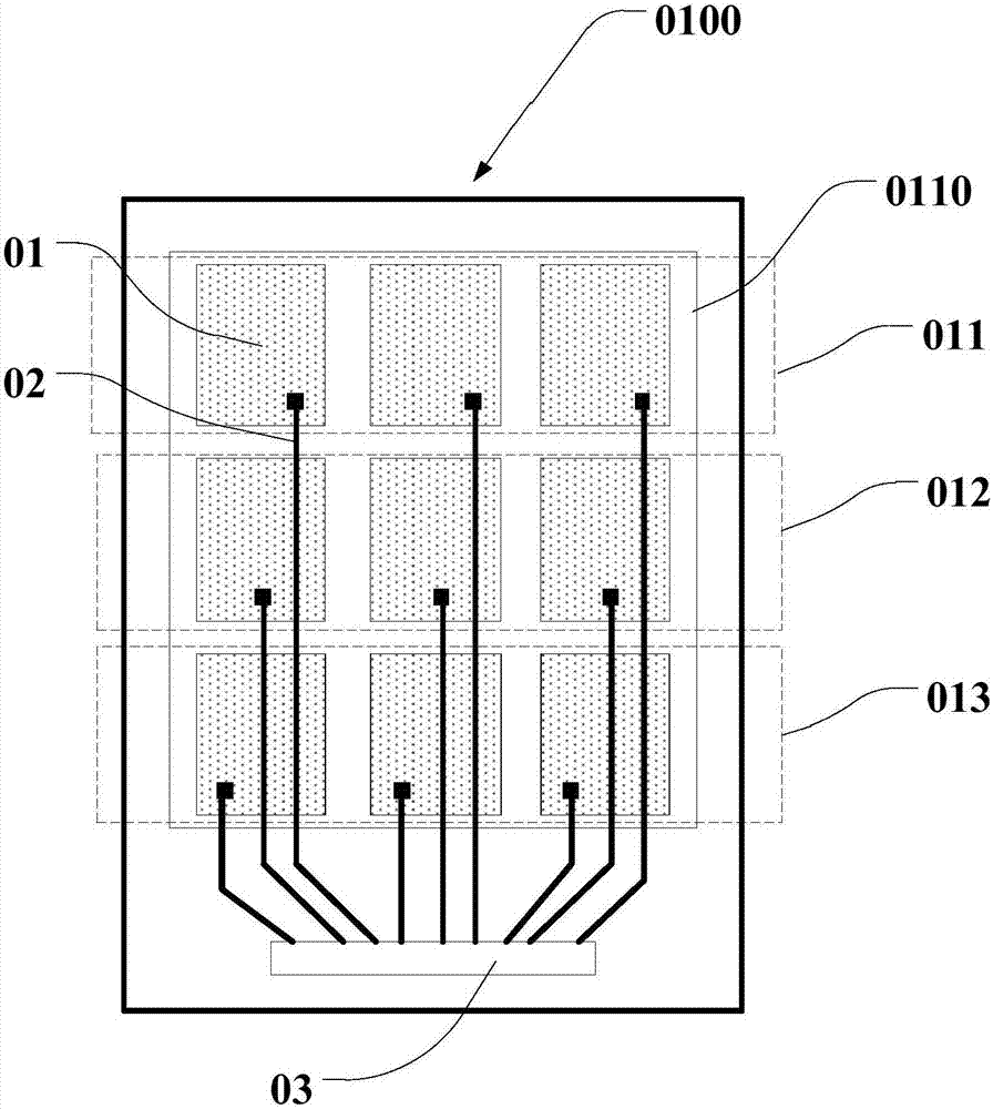
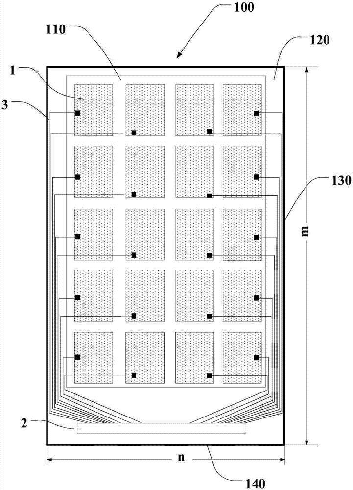
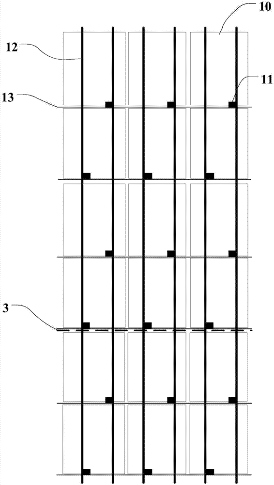
[0044] like figure 2 and image 3 As shown, the array substrate 100 provided by the embodiment of the present invention includes a display area 110 and a non-display area 120. The display area 110 is provided with a plurality of pixel units 10 arranged in an array, and thin film transistors corresponding to the plurality of pixel units 10 one-to-one. 11. A plurality of data lines 12 and a plurality of scanning lines 13 arranged in an insulating cross, and a plurality of touch electrodes 1 arrang...


PUM


Abstract

The invention discloses an array substrate, a touch control panel and a touch control displayer. According to the technical purposes, the difference of the capacitance when touch control electrodes of the touch control display panel are interfered is reduced, and the touch control precision of the touch control display device is improved. The array substrate in the embodiment comprises a display area and a non-display area, the display area is provided with a plurality of pixel units arranged in an array mode, thin film transistors which correspond to the pixel units one to one, a plurality of data lines, a plurality of scanning lines and the touch control electrodes, wherein the data lines and the scanning lines are arranged in an isolated and crossed mode, and the touch control electrodes are arranged in an array mode. The non-display area is provided with a drive chip, and each touch control electrode is connected with the drive chip through at least one touch control signal line, wherein the relation between the length m of the array substrate in the extending direction of the data lines and the length n of the array substrate in the extending direction of the scanning direction meets the relational expression, namely m:n >=2:1, and the touch control signal lines extend to the non-display area in the extending direction of the scanning lines and are connected to the drive chip along the non-display area.

Description

technical field [0001] The present invention relates to the field of display technology, in particular to an array substrate, a touch display panel and a touch display device. Background technique [0002] With the rapid development of display technologies, touch screens have gradually permeated people's lives. At present, touch screens can be divided into: resistive, capacitive, infrared, surface acoustic wave, electromagnetic, vibration induction, frustrated total internal reflection optical induction, etc. according to the working principle. Among them, the capacitive touch screen is generally sought after by the industry because of its unique touch principle, high sensitivity, long life, high light transmittance and other advantages. [0003] At present, most capacitive touch screens are plug-in, that is, the touch panel and the display panel are manufactured separately and then bonded together. This technology has the disadvantages of high production cost, low light t...

Claims


Application Information

Patent Timeline
Patent Type & Authority Applications(China)
IPC IPC(8): G02F1/1333H01L27/32G06F3/041
CPCG02F1/13338G06F3/0412H10K59/40
Inventor 席克瑞秦锋张敏周九斌崔婷婷
Owner SHANGHAI AVIC OPTOELECTRONICS
Why Eureka
Try Eureka