Substrate, semiconductor package including substrate, and manufacturing method thereof
A technology for substrates and conductive elements, which is applied in the field of manufacturing the substrates, and can solve the problems of long transmission paths and large areas of electrical signals
- Summary
- Abstract
- Description
- Claims
- Application Information
AI Technical Summary
Problems solved by technology
Method used
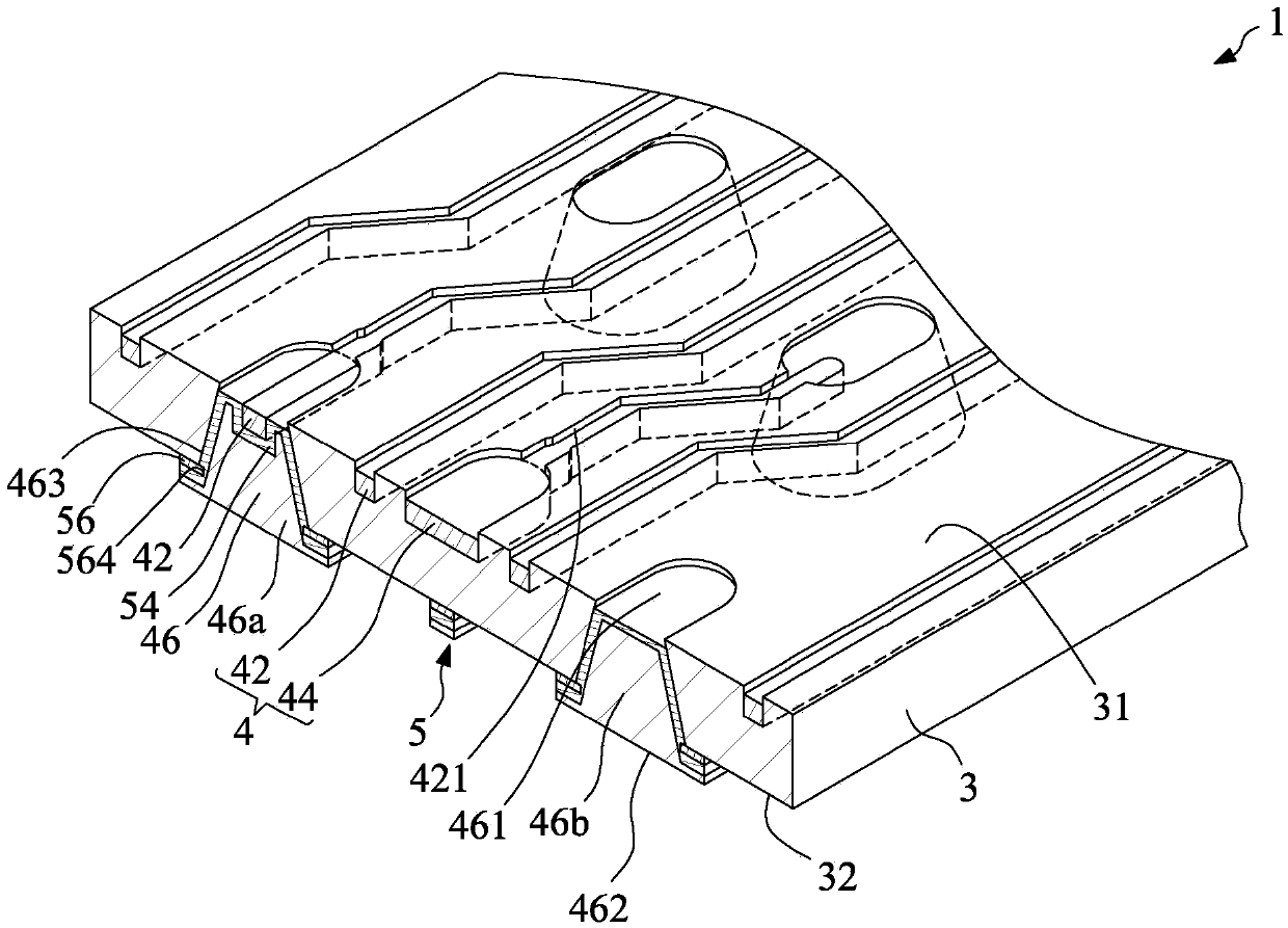
Image


Examples
Embodiment Construction
[0045] In the drawings and detailed description, common reference numerals are used to designate the same or similar components. Embodiments of the present invention will be readily understood from the following detailed description taken in conjunction with the accompanying drawings.
[0046] The following disclosure provides many different embodiments, or examples, for implementing different features of the provided subject matter. Specific examples of components and arrangements are described below to illustrate certain aspects of the invention. Of course, these components and arrangements are examples only and not limiting. For example, in the following description, a first feature formed over a second feature may include embodiments in which the first feature is formed or disposed in direct contact with the second feature, and may also include embodiments in which additional features may be formed or disposed over the second feature. An embodiment between a feature and ...
PUM
 Abstract
Description
Claims
Application Information
 - R&D
- Intellectual Property
- Life Sciences
- Materials
- Tech Scout
- Unparalleled Data Quality
- Higher Quality Content
- 60% Fewer Hallucinations
Browse by: Latest US Patents, China's latest patents, Technical Efficacy Thesaurus, Application Domain, Technology Topic, Popular Technical Reports.
© 2025 PatSnap. All rights reserved.Legal|Privacy policy|Modern Slavery Act Transparency Statement|Sitemap|About US| Contact US: help@patsnap.com