Dividing method and device of memory space of flash memory in field-programmable gate array
A storage space and gate array technology, applied in the direction of input/output to record carrier, etc., can solve the problems of increasing the cost of FPGA system, restricting the convenience and flexibility of FPGA data storage, and waste of space, so as to improve convenience and flexibility , Avoid space waste and reduce cost
- Summary
- Abstract
- Description
- Claims
- Application Information
AI Technical Summary
Problems solved by technology
Method used
Image

Examples
Embodiment Construction
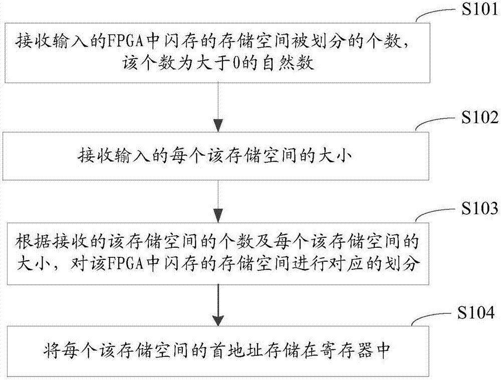
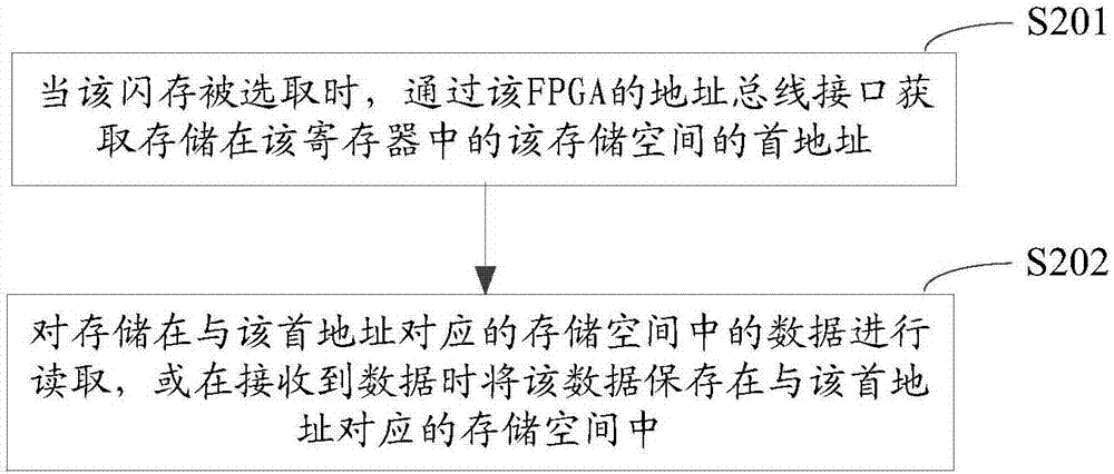
[0046] In order to make the objectives, technical solutions and advantages of the present invention clearer, the present invention will be further described in detail below with reference to the accompanying drawings and embodiments. It should be understood that the specific embodiments described herein are only used to explain the present invention, but not to limit the present invention.
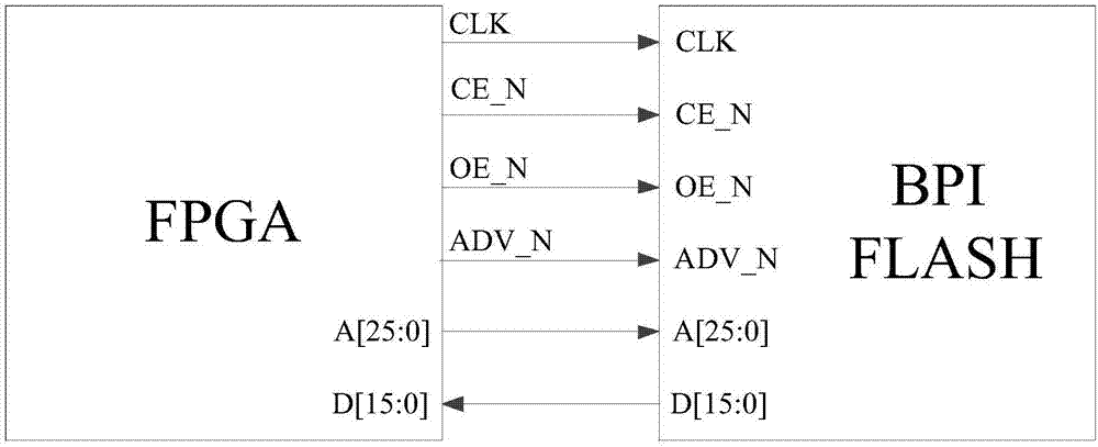
[0047] figure 1 For the connection schematic diagram of field programmable gate array FPGA and flashing memory FLASH according to an embodiment of the present invention, below in conjunction with figure 1 To describe in detail the connection relationship between the Field Programmable Gate Array FPGA and the flash memory FLASH according to an embodiment of the present invention, as figure 1 As shown, FPGA and parallel FLASH are interconnected, where:
[0048] The clock output port CLK of the FPGA is connected to the clock input port of the parallel FLASH;
[0049] The chip select output...
PUM
 Abstract
Description
Claims
Application Information
 - R&D
- Intellectual Property
- Life Sciences
- Materials
- Tech Scout
- Unparalleled Data Quality
- Higher Quality Content
- 60% Fewer Hallucinations
Browse by: Latest US Patents, China's latest patents, Technical Efficacy Thesaurus, Application Domain, Technology Topic, Popular Technical Reports.
© 2025 PatSnap. All rights reserved.Legal|Privacy policy|Modern Slavery Act Transparency Statement|Sitemap|About US| Contact US: help@patsnap.com