Flexible display device

A display device, a flexible technology, applied in the direction of electrical components, electric solid devices, circuits, etc., can solve the problems of difficult reduction of line width and line spacing in non-display areas, difficulty in reducing the width of non-display areas, poor adhesion, etc.

Active Publication Date: 2018-01-12
E INK HLDG INC
View PDF3 Cites 4 Cited by
  • Summary
  • Abstract
  • Description
  • Claims
  • Application Information

AI Technical Summary

Problems solved by technology

Since the buffer layer is generally made of organic materials, and the circuit layer is generally made of metal materials, when the circuit layer is formed above the buffer layer, there will be a problem of poor adhesion between the circuit layer and the buffer layer
[0003] When the flexible display device is bent due to force, the circuit layer is displaced due to the poor adhesion of the circuit layer above the buffer layer
As a result, the circuit layer on the buffer layer is prone to fracture due to flexing
In addition, in the wet etching process, the circuit layer on the buffer layer of the non-display area is also prone to the problem of excessive critical dimension change (CD loss)
Therefore, it is difficult to reduce the line width and line spacing of the non-display area, making it difficult to reduce the width of the non-display area

Method used


Image

  • Flexible display device
  • Flexible display device
  • Flexible display device

Examples


Embodiment Construction

[0022] A number of implementations of the present invention will be disclosed below with the accompanying drawings. For the sake of clarity, many practical details will be described together in the following description. It should be understood, however, that these practical details should not be used to limit the invention. That is, in some embodiments of the present invention, these practical details are unnecessary. In addition, for the sake of simplifying the drawings, some well-known and commonly used structures and elements will be shown in a simple and schematic manner in the drawings.

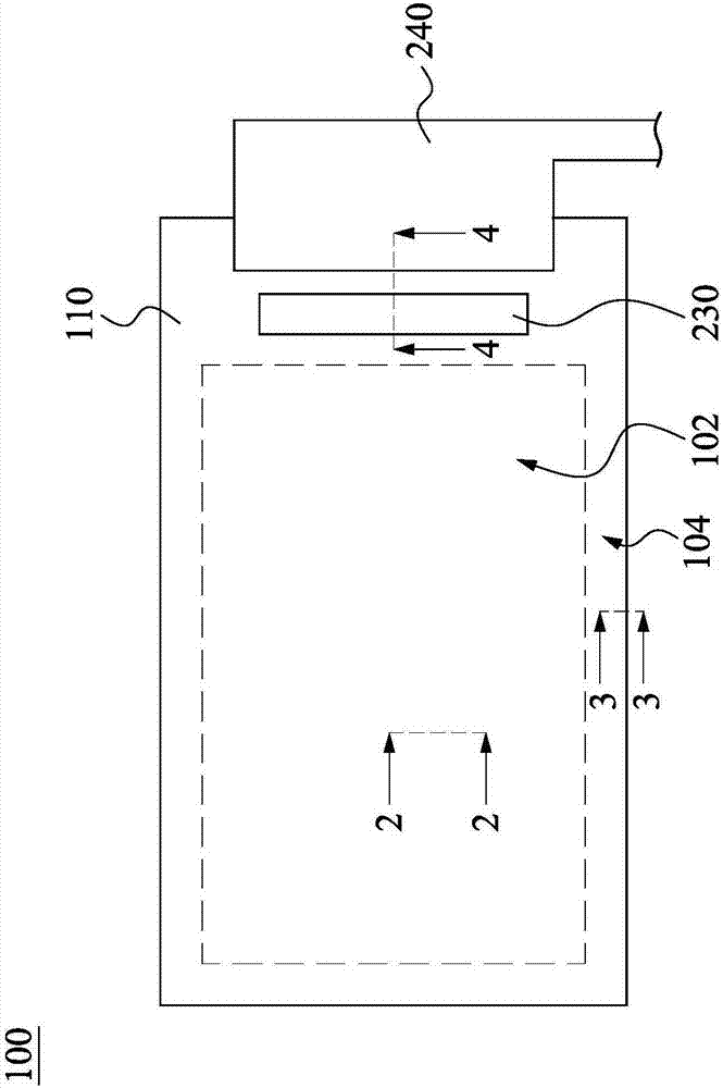
[0023] figure 1 A top view of the flexible display device 100 according to an embodiment of the present invention is shown. The flexible display device 100 has a display area 102 and a surrounding area 104 , and the surrounding area 104 surrounds the display area 102 . as the picture shows, figure 1 The inside of the dotted line is the display area 102 , and the outside of the dotte...


PUM

PropertyMeasurementUnit
thicknessaaaaaaaaaa

Abstract

A flexible display device includes a flexible substrate, an inorganic barrier layer, a metal layer, an organic buffer layer, and an insulating layer. The inorganic barrier layer is located on the flexible substrate. The metal layer is located on the inorganic barrier layer and in contact with the inorganic barrier layer. The organic buffer layer covers the inorganic barrier layer and the metal layer, and has at least one conductive via connected to the metal layer. The insulating layer is located on the organic buffer layer. Since the metal layer is non-organic material, it allows excellent adhesion between the metal layer and the inorganic barrier layer. When the flexible display device is bent due to the force, the metal layer is less likely to be broken by bending.

Description

technical field [0001] The invention relates to a flexible display device. Background technique [0002] When fabricating a flexible display device with an organic thin film transistor (Organic Thin Film Transistor; OTFT), a barrier layer, a buffer layer and a circuit layer may be sequentially formed on the flexible substrate. Since the buffer layer is generally made of organic material, and the circuit layer is generally made of metal material, when the circuit layer is formed above the buffer layer, there will be a problem of poor adhesion between the circuit layer and the buffer layer. [0003] When the flexible display device is bent due to force, the circuit layer above the buffer layer is displaced due to poor adhesion. As a result, the circuit layer on the buffer layer is easily broken due to bending. In addition, in the wet etching process, the circuit layer on the buffer layer of the non-display area is also prone to the problem of excessive critical dimension cha...

Claims


Application Information

Patent Timeline
Patent Type & Authority Applications(China)
IPC IPC(8): H01L27/32H01L27/12
Inventor 林冠峄陈昱文洪裕杰卢俊宇
Owner E INK HLDG INC
Why Eureka
Try Eureka